Surface enhanced Raman spectroscopy (SERS) has gained considerable attention recently because of the increasing interest in the field for applications like food safety, environmental safety and homeland security. There has been a significant increase in the number of SERS publications globally from 3000 to 25000 between 2000 and 2011.
The drive for SERS technology development is based on the need to overcome the technical barrier of the lower detection limit with Raman spectroscopy and also the need for trace level detection of chemical residuals, explosive compounds and biomedical diagnostics.
It is extensively believed that surface enhancement mechanisms are due to either electromagnetic resonances between the collective plasmon oscillations in metal particles and the incident optical field or because of chemical enhancement via the increase of molecule polarization after combining with the metal surface.
With nanotechnology advancements, SERS technology has reached an era where SERS chips are fabricated with highly controlled nanostructures on a substrate using gold or silver metals. Another SERS type is solution-based, which uses colloidal silver or gold particle solutions.
Raman Instrumentation for SERS
For SERS end users and SERS developers interested in a particular SERS application, the focus of their technological or experimental platform must be a Raman setup offering consistent lab grade performance, is portable and affordable, enabling them to tackle practical problems.
The latest dispersive portable Raman spectrometer series has brought SERS closer to practical applications. Since the SERS substrate area (~5x5mm2) is small where a tiny sample solution droplet is deposited, precise laser focusing on the surface is mandatory for Raman instrumentation.

Figure 1. Illustration of a Raman Measurement Using a SERS Chip
While benchtop microscopic Raman systems satisfy this need, they are not portable. This hinders SERS developers from transferring their technologies to environments like field testing, production lines or diagnostic locations where SERS analysis needs to be carried out. The increased cost of a benchtop micro-Raman restricts the adoption of SERS for practical applications.
The ideal setup for SERS analysis is a B&W Tek i-Raman Plus portable Raman system combined with a BAC151video microscope sampling accessory in a BAC152 laser Class 1 enclosure. For solution-based SERS, in case the measurement is performed directly via the solution vial, it is possible to use the BCR100A Raman cuvette holder with the i-Raman Plus.

Figure 2. B&W Tek i-Raman Plus portable Raman system, BAC151video microscope sampling accessory, BAC152 laser Class 1 enclosure and BCR100A
High Signal to Noise Ratio for Best Limit of Detection
The highlight of the B&W Tek i-Raman Plus is a back-thinned CCD detector with TE-cooling to -2°C. In comparison with a traditional front-illuminated CCD with quantum efficiency at 50%, it is possible for the back-thinned CCD quantum efficiency to reach up to 90%.
Since the Raman phenomenon has a low efficiency (10-8), it is essential that the CCD detector electronic noise is very low compared to the Raman signal. The noise is effectively reduced due to TE-cooling of the CCD device. The dark noise reduces by 50% for each 7°C decrease in device temperature.
The cooled i-Raman Plus detector enables very long integration times of up to 30 minutes. This considerably improves the detection limit and makes low-light level applications such as SERS possible. For fluorescence detection, the 785nm laser wavelength must be used.
High Resolution to Resolve Peaks of the Substrate and the Sample
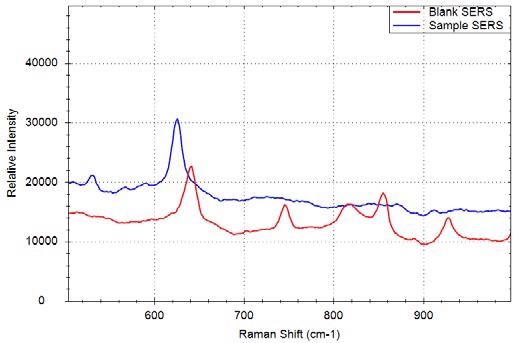
There are intrinsic Raman peaks from the blank SERS surface for certain SERS chips. When the Raman peaks from the sample material are close to the peaks from the blank SERS substrate, it is critical that the sample Raman peaks be separated from the peaks of the SERS chip.
The spectral resolution for the i- Raman Plus system is 4.5cm-1, which offers sufficient resolving capability for differentiating two closely positioned peaks. Figure 3 shows two closely located peaks, with one peak (641cm-1) associated with the blank SERS and one peak (625cm-1) related to the sample solution improved by SERS.

Figure 3. Raman Spectra of a blank SERS surface (red) and a sample material on SERS
Small Laser Beam Size and Accurate Focusing Control
Since SERS chips are very small in size, precise laser focusing control and a small laser beam size are required. The sampling accessory of the BAC151 video microscope combined with the i-Raman Plus provides a laser beam size from 26 to 420µm when objective lenses having a range of magnifications are used. The working distance and laser beam size when the objective lens magnification changes from 5X to 80X is shown in Table 1.
Table 1. Laser Spot Size from BAC151
| Objective Lens Magnification |
Working Distance (mm) |
Laser Spot Size (µm) |
| 5X |
26.1 |
420 |
| 10X |
20.2 |
210 |
| 20X |
8.80 |
105 |
| 40X |
3.98 |
52 |
| 50X |
3.68 |
42 |
| 80X |
1.25 |
26 |
Laser Safety and Blocking of Ambient Light Interference
Since several types of SERS chips generate specular reflective light when the excitation laser beam is directed on to the SERS surface, it is important to have an enclosure which can shield off the reflected laser beams and also block interference from ambient light. The BAC152 offers a laser Class 1 enclosure for laser safety and also for the required blocking of ambient light.
Conclusions
The B&W Tek i-Raman Plus portable Raman system combined with a BAC151video microscope sampling accessory inside a BAC152 laser Class 1 enclosure offers a suitable setup for SERS applications. The setup offers not just a high S/N ratio for best detection limit and high resolution to resolve peaks, but also provides a tiny and adjustable laser beam size along with precise focusing control. Finally the laser Class 1 enclosure offers the required laser safety and also eliminates ambient light interference.

This information has been sourced, reviewed and adapted from materials provided by B&W Tek.
For more information on this source, please visit B&W Tek.