Testing the hardness of micro materials is a task that requires special equipment and high skill levels. Nanoindentation is a fast, easy and accurate technique to test microhardness as compared to traditional testing methods. This is because the size of the indentation is determined directly from the relationship between force and penetration depth, both of which are measured continuously. From this data, material properties can be derived, such as elastic modulus and hardness.
Using the software NanoBlitz 3D helps enable fast and accurate mapping of mechanical material properties by nanoindentation. The indentations take place in 0.6 seconds and produce a grid automatically using the software.
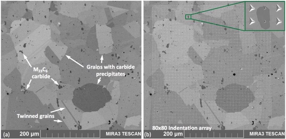
Figure 1. SEM image of a polished polycrystalline Nibase superalloy. The complex microstructure has a polycrystalline structure, including twin grain boundaries and a high number of M23C6 carbides. The grain boundaries of the alloy are continuously occupied by carbide precipitation.
The region shown in Figure 1 was tested with the NanoBlitz 3D method. The testing used a grid of 80 x 80 indentations, for a total of 1600 indentations. The distance between the indents is 5 microns. The resulting grid is shown in Figure 1b. Each grid point includes information on the rigidity, hardness, and elastic modulus of the material. From this data, the desired material properties can be displayed in a property map.
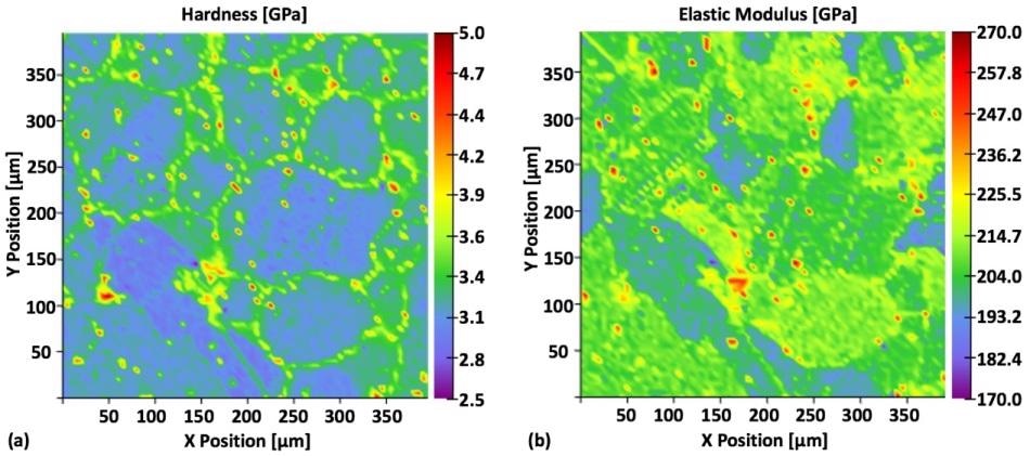
Figure 2. Hardness (a) and elastic modulus (b) property maps. The inter-granular carbide is difficult to discern from the SEM image, but clear in the hardness map, where the carbide precipitation appears yellowish. The map of elastic modulus provides information on the elastic properties of the respective phases and grain orientation.

This information has been sourced, reviewed and adapted from materials provided by Nanomechanics, Inc.
For more information on this source, please visit Nanomechanics, Inc.