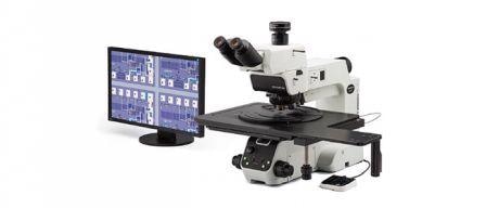
For quality control purposes, wafers, such as semiconductor or flat-panel display (FPD) chips, need to be examined under a microscope to verify that they meet specifications related to both circuit pattern and color. With a conventional microscope, brightfield illumination is used to observe the color of the wafer and darkfield illumination to view the circuit pattern. To compile a complete quality control report on a wafer, acquiring images with each of these techniques is necessary, with repeated switching back and forth between them. Consequently, generating quality control reports for wafers using conventional microscopy is time-consuming and inefficient.
The Solution from Evident
MX63 and MX63L industrial microscopes feature a MIX illumination setting that combines brightfield and darkfield images in one image (Figure 1). This function provides a quick and efficient method of inspecting FPD and semiconductor chips as the color and the circuit pattern can be observed at the same time, with high resolution, sharpness, and clarity. The time it takes to generate a report is drastically shorter.

Figure 1. Integrated circuit pattern on a semiconductor using darkfield (left) and MIX (brightfield + darkfield) illumination (right). MIX illumination enables observation of patterns, colors, and minute scratches or flaws.
Another application of MIX illumination for semiconductors is the detection of contamination and photoresist residue on wafers. Using MIX illumination of fluorescence and darkfield, the circuit pattern and photoresist residue can be easily observed as depicted in Figure 2.

Figure 2. Photoresist residue on a semiconductor wafer observed using fluorescence (left) and MIX (fluorescence + darkfield) illumination (right).
Other observation methods available on MX63 and MX63L microscopes for wafer inspection are polarized light and differential interference contrast (DIC). For inspections of wafer and liquid-crystal display (LCD) structures, polarized light can be utilized to elucidate the material’s texture and crystal condition. DIC can aid in wafer inspection by showing miniscule height differences, such as magnetic heads, hard-disk media, and polished wafers.
Product Features
The MX range of industrial microscopes offer several advantages including the following:
- A smoother workflow from beginning to end, enabled by multiple visualization-enhancing functions and excellent optical performance that remains unchanged in a cleanroom setting
- Simple, easily adjustable settings, such as the focus, light intensity, and aperture size, supported and assisted by the microscope’s software. Even technicians with relatively little experience can produce high-quality observations following inspection.
- Excellent clarity and sharp focus for highly accurate measurements, stemming from Evident’ decades-long experience in building high-quality optical imaging instruments
- A modular design with a wide range of components and accessories offering the possibility to a customize the microscope to the specific needs of the user, without a major investment
Products Used

MX 63 and the MX 63L microscopes provide reliable observation of wafers up to 300 mm in size, as well as printed circuit boards, flat panel displays, and other large parts with circuitry. Flexible functionality, as well as an ergonomic design with intuitive controls, make MX63 and MX6L microscopes both comfortable and easy to use. The modular design enables users to design systems to observe a range of objects under optimal conditions. When MX63 and MX6L microscopes are used with Stream™ and PRECiV™ image analysis software, the inspection procedure can be simplified and certain settings automated, so the complete process is faster and more efficient, from observation to final report creation.

This information has been sourced, reviewed and adapted from materials provided by Evident Corporation - Industrial Microscopy.
For more information on this source, please visit Evident Corporation - Industrial Microscopy