Sponsored by HORIBAJun 14 2018
SEM-CathodoLuminescence (SEM-CL) is a technique in which photons possessing specific wavelengths are emitted from a material which is bombarded by high-energy electrons, these being generated by an electron gun in a scanning electron microscope. This method works in different ways depending on the composition, the lattice structure or if there is any strain or damage resulting in altered structure.
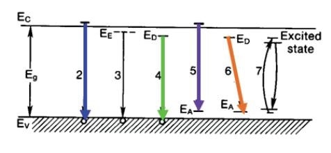
The occurrence of such luminescence has a theoretical basis in the solid-state band theory. A solid insulator such as calcite or quartz may be understood to have a valence electronic band as well as a conduction band that is interrupted by a band gap called the forbidden gap.
If a crystalline structure is hit by electrons with energy sufficient to promote lower-valence band electrons to a conduction band with higher energy, the promoted electrons return to the valence band in the ground or non-excited state almost instantaneously. However, they may be retained for a very brief period, measured in microseconds, in the presence of intrinsic or extrinsic impurities, such as defects in the material structure and traps, respectively.
Once the electrons are released from these traps, they emit energy which may cause luminescence if it is within the required range of energy or wavelength. Many light photons are within the visible part of the electromagnetic spectrum, corresponding to a wavelength of 400-700 nm. However, some are within the ultraviolet or infrared regions.
The production of luminescence by the interaction of traps occurs in many ways. Excited energetic electrons promoted to the conduction band may return to the ground state without being trapped, or they may display random motion throughout the crystal structure until they enter a trap.
Afterwards they may either return to the ground state at once or enter more traps, emitting light of different wavelengths depending on the difference in energy at each step. Thus, the cathodic luminescence (CL) shows intensity in proportion to trap density.
Photon energy < EGap
Recombination with impurity
eA0 : electron in CB – hole of neutral acceptor
D0h : electron of neutral donnor – hole in VB
DAP : electron of neutral donnor – hole of neutral acceptor
What are the main differences between optical-CL (cold cathode) and SEM-CL?
The basis of the most frequently used optical-CL setup is the cold-cathode CL, attached to a conventional optical microscope so that the same area of the specimen can be examined optically as well as with CL.
Here a discharge at high negative voltage occurs between the anode and cathode at ground potential, in ionized gas, within a vacuum of about 10-2 Torr (while conventional SEMs require a vacuum of 10-5 or more), which results in an electron beam. This leads to a low-level CL in the majority of materials that have CL properties.
The luminescence is viewed using the objective lens of the optical microscope, or a digital camera is used to record the image.
The emission of cold-CL gives information about the presence of trace elements within minerals or about defects induced by mechanical means within crystals. Geological studies are aided by seeing the pattern of CL within a material, helping to understand the way a crystal grows, and the presence of lattice replacement, crystal deformation and the geographical origin of the crystal. Some limitations exist with the use of optical-CL to acquire CL images rather than SEM-CL, such as:
- Poor image magnification
- Optical-CL images are generated only within the visible light region
- Lower resolution
- More time needed for image acquisition and processing
What is SEM-Raman?
Raman spectroscopy is another method of chemical analysis based upon light scattering by a material, which leaves the sample intact while yielding a wealth of information on the structure, phase and polymorphous nature of the specimen, in addition to its crystalline nature and molecular interactions. It analyzes the material on the basis of how light interacts with the chemical bonds inside a material, as the molecule scatters the incident light emitted by a laser light source of high intensity.
Light scattering results mostly in photons having the same wavelength as the emitted light from the laser source. This is called Rayleigh scatter and does not give much data on the specimen. Some light, about 0.0000001%, is scattered and this results in photons with different colors from the original light. This is the Raman effect, and is specific for the chemical structure of the substance analyzed.
SEM-Raman measurement uses Raman spectroscopy inside the specimen chamber of the electron microscope. For this to happen, the excitation laser is directed on the sample in a vacuum. The resulting Raman spectrum is characterized by several peaks, which show the different wavelengths as well as intensities of the light that has undergone Raman scattering.
Each of the different peaks is specific for every type of vibrational bond movement within a molecule. This includes both individual bonds such as C-C, C-H, N-O, and C=C, and bond clusters such as polymer chain, lattice modes, or the breathing mode of a benzene ring.
Why are Raman spectroscopy, PL, and CL complementary techniques?
The use of Raman spectroscopy, PL and CL on the same sample, whether a mineral, semiconductor or ceramic, or even a novel 2D material, gives data on different aspects of the molecules which help to achieve a comprehensive understanding of the analyte’s structure.
CL and PL are important in the study of bandgaps in luminescent materials, defects in crystal growth and impurities, and a variety of excitotonic recombination pathways, while Raman spectroscopy helps understand the chemical structure and other characteristics such as the identity, polymorphous nature, stress or strain on the structure, phases, and contaminants.
The latter thus provides a specific spectral pattern often called a chemical fingerprint, which identifies a molecule or material or helps pick it out from others.
A library of thousands of Raman spectra is useful to rapidly match the identity of a material with its Raman spectrum. Electron beam excitation in SEM-CL proves superior to SEM-Raman and SEM-PL in the ability to achieve excellent resolution to a range of a few tens of nanometers with the scanning electron microscope, compared to nanometer-scale resolution with the use of a scanning transmission electron microscope.
SEM-PL and SEM-Raman, in contrast, achieve resolution only up to the micrometer scale, due to the presence of optical diffraction.
What are the most common applications of SEM-CL?
Semiconductors that show a direct bandgap, such as GaAs or GaN, are ideal for analysis by SEM-CL techniques, but those such as silicon with an indirect bandgap are also capable of showing weak CL and may be subjected to this type of analysis.
Dislocated and intrinsic silicon are noted to have different luminescence, and this fact is taken advantage of to map the location of defects in integrated circuits. A recent development is the use of CL within an electron microscope to generate surface plasmon resonances in nanoparticles of metal for analysis.
The importance of surface plasmons in such nanoparticles is their ability to absorb and emit light, but the way in which this takes place is quite different from the process in semiconductors. CL can be used in a probe to map the distribution of density in different states of photonic crystals in a planar dielectric state, as well as photovoltaic nanomaterials.
SEM-CL is also used to study minerals and in geologic applications such as:
- Studying how diagenesis and cementation occur in sedimentary rock strata.
- Establishing the formation of clastic material within metasedimentary and sedimentary rock.
- Analyzing the detailed internal anatomy of fossils.
- Study of growth and dissolution in metamorphic rocks and igneous minerals.
- Finding how metamorphic rock undergoes deformation.
What are the advantages of SEM-CL?
Sensitivity
SEM-CL is very sensitive and thus detects variations in the chemical nature of a substance at a lower level than can be detected by X-ray analysis. This gives it an edge over conventional SEM-EDX and SEM-WDX testing when it comes to detecting traces of rare earth elements. It is also extremely sensitive to alterations in temperature, chemical makeup, crystal structure, defects in the structure and any structural strain. This also makes it difficult to interpret, however.
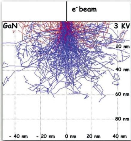
Monte-Carlo simulation of electron paths
High Spatial Resolution
Molecular interactions occur within a part of the specimen that varies with factors such as:
- Increased angle of incidence of the electron beam reduces the volume of interacting molecules.
- The higher the atomic number, the greater the absorption of electrons.
- The higher the accelerating voltage that is applied to the electron beam, the deeper it penetrates and the larger the volume of interaction.
What are the most common applications of SEM-Raman spectroscopy?
SEM-Raman is used to study the structure and purity of carbon and 2D materials, including nanotubes, hBN, graphene, MoS2, any defect or disorder in structure.
It is also employed to analyze various characteristics of the following classes of material:
- Semiconductors – their purity, the composition of the alloy composition, the presence of intrinsic stress/strain.
- Geology – the ability to identify minerals and analyze their distribution, detect fluid inclusions, and phase transitions.
- Art and Archaeology – to describe the typical features of paints and pigments, ceramic materials, and precious stones.
- Pharmaceutics – to test for homogeneous content and even distribution of the constituents.
What type of CL image acquisition is used?
CL Panchromatic image is typically a grayscale image where the light intensity emitted for each pixel is collected as a single band of data by the detector. This is described as integrated intensity. A PMT photomultiplier is connected directly to the interface of the CL which collects the data and this detects the light.
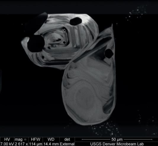
Zircon sample
CL RGB image is an image combining multiple spectra, comprising the three visual bands of primary colors (red, green and blue). The connection between the three bands gives a “true color” image.
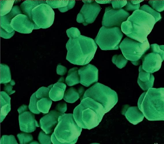
Phosphor image
CL hyperspectral image consists of an image in which each pixel has a whole spectrum. An electron beam is used to scan the sample across for small mapping, each area covering a few hundred micrometers, while a whole spectrum is obtained for each point. The light is collected using a spectrometer fitted with a CDD detector.
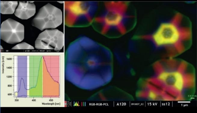
Hyperspectral image

This information has been sourced, reviewed and adapted from materials provided by HORIBA.
For more information on this source, please visit HORIBA.