In this interview, AZoM talks to Dr. Thomas Luxbacher about the semiconductor industry, how surface charge analysis plays an important part, and how Anton Paar is impacting the field.
Please could you give a brief overview of how surface charge analysis can be beneficial in the semiconductor field?

Image Credit: Anton Paar GmbH
When we refer to surface charge analysis, we consider the charge at the interface between a material and a surrounding aqueous solution.
With respect to the semiconductor field, knowing the charge at the wafer-water interface is extremely important for processes like chemical etching, wafer cleaning and chemical-mechanical planarization (CMP).
The CMP process involves not only the interaction of a wafer surface with solutes such as an acid, a base, or a surfactant but also with dispersed slurry particles.
Surface charge is the initiator of electrostatic forces between the wafer surface and these solutes or suspended particles. The interfacial parameter that drives the electrostatic interaction is known as the zeta potential. It is related to the charge density and accepted as a representative indicator for surface charge, which otherwise is difficult to determine.
The nature of the surface charge and the location of the zeta potential at the solid-water interface render this parameter not only dependent on the surface chemistry of the solid material but also on the composition of the aqueous surrounding, especially the pH and the salinity of an aqueous solution determine the sign and magnitude of the zeta potential of a given material.
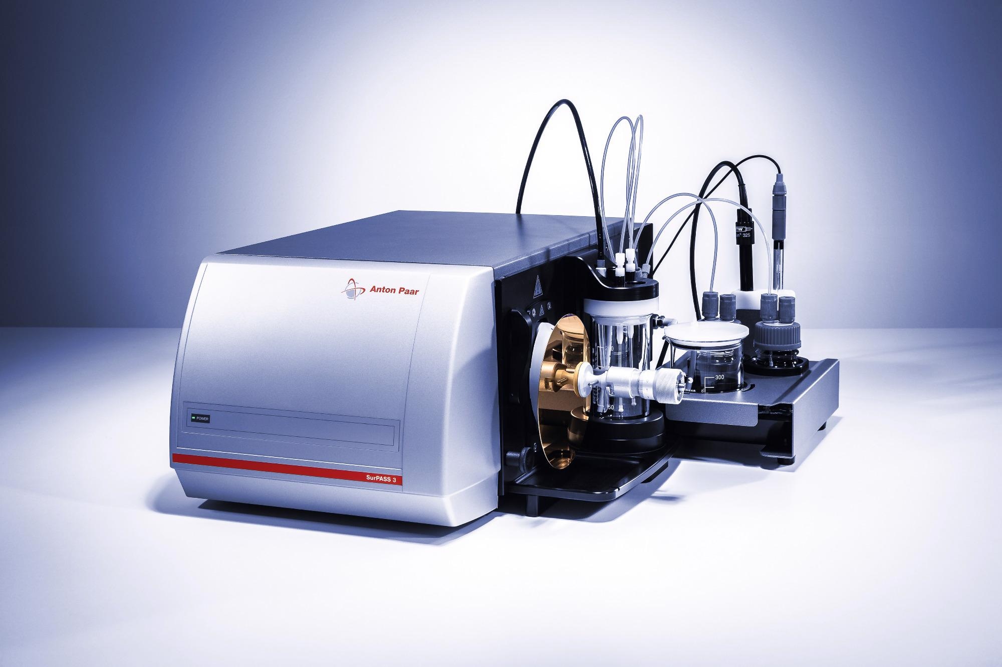
The surface charge and zeta potential can be measured with Anton Paar’s SurPASS 3.
What are the key challenges in semiconductor production that can be met with zeta potential analysis?

Image Credit: Anton Paar GmbH
Let us again consider the CMP process: The wafer and the CMP slurry particles assume their respective charge and electrostatic forces dominate the wafer-particle interaction.
In order to keep CMP slurry particles off the wafer surface, process conditions that favor electrostatic repulsion are desirable. Measurement of the zeta potential of both a wafer surface and a slurry particle permits prediction of the effectiveness of a CMP process.
When tuning the composition of the slurry, it is possible to reduce the adsorption of slurry particles on a wafer surface.
The zeta potential analyses for both slurry particles and wafers with different top coatings assist slurry manufacturers in the development of application-specific formulations and wafer fabs in the selection of slurries appropriate for their wafers.
Particle-surface interactions are not restricted to the semiconductor wafer. Consider the CMP pads, which must not transfer particles from one wafer to the other to eliminate cross-contamination. In the cleaning process, brushes made of PVA are also attractive to particle deposition.
The information provided by the zeta potential at the interface between the polymeric materials of pads and brushes and the corresponding solutions supports the taking of measures to avoid unfavorable contamination.
How is the zeta potential determined for slurry particles and wafer surfaces?
Two different methods are necessary to assess the zeta potential for slurry particles and large material surfaces. Particles in dispersion, such as a CMP slurry are considered a colloidal sample, and the method of choice is electrophoretic light scattering (ELS), which can be applied with the Litesizer 500 .
In ELS, an electric field is applied on a particle dispersion, which drives the charged particles to move towards the corresponding electrode. The particle mobility is measured indirectly by recording the intensity and frequency shift of the scattered light of a laser beam.
For large solid samples, such as semiconductor wafers, a different though analogous technique is employed: measurement of the streaming potential. This can be done with SurPASS 3.
In this method, the solid sample is arranged in such a way as to provide a capillary flow channel. A pressure gradient is applied on a test solution, which compels this liquid to flow through the capillary channel. The liquid flow creates an electric potential, which is recorded as the streaming potential.
Although these two techniques produce completely different raw signals, the calculated zeta potential has a single theoretical origin and the results obtained by electrophoretic light scattering and streaming potential measurement become comparable.
Anton Paar offers instruments that cover both methods for the zeta potential analysis, namely Litesizer 500 and SurPASS 3.
How can I imagine the creation of a flow channel for a semiconductor wafer?
In principle, the solution is straightforward. You need two pieces of the same sample and then you align the flat active surface layers opposite each other, thereby separating the samples by a small capillary distance.
Usually, this approach requires cutting the sample, for example, to a size of 1-2 cm2. Since this is undesirable for subsequent use of the same sample for other analytical techniques or further processing steps, a sample holder for SurPASS 3 is available for the non-destructive zeta potential analysis of semiconductor wafers, but also other solid samples such as sensor chips or EUV masks for state-of-the-art lithography.
The small but acceptable drawback of this sample holder is the requirement to use a reference sample that completes the flow channel, i.e., one side of the channel is comprised of the sample, such as a wafer, and the opposite side faces the reference, preferably an already built-in high grade polymer.
Does Anton-Paar also provide other instruments for wafer production?

Image credit: Anton Paar
Anton Paar provides wafer metrology tools for monitoring the quality of thin films, understanding the surface chemistry of outer layers and characterizing wafer defects.
Our instruments help determine and adjust many different parameters throughout the wafer manufacturing process - from thin films to testing, assembly and packaging - to create a better end product.
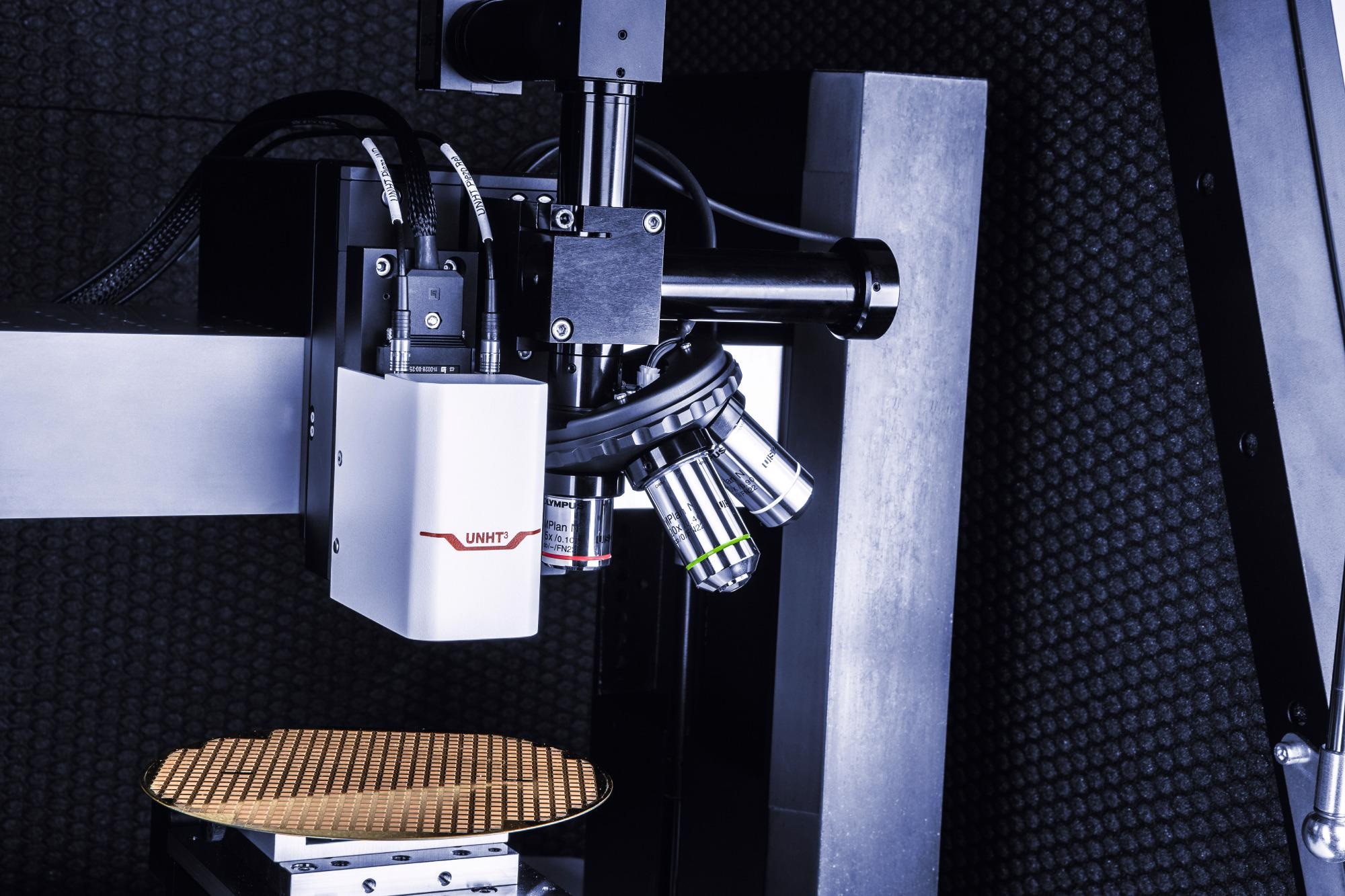
For the mechanical surface characterization of wafers, Anton Paar offers two state-of-the-art measuring technologies, namely scratch testing and instrumented indentation testing.
Density and concentration measurement is important to determine the correct concentration of the etching substance, which is key to obtaining consistent etching results with the highest precision. Anton Paar also provides instruments for SAXS, particle analysis, solid density analysis and microwave digestion.
What aspects of the production process do you think could be improved and how could Anton Paar help with this?
Measuring certain parameters during the production process means controlling them and being able to react to changes, as well as designing the raw materials and processes to reach the highest possible efficiency and product quality.
Nanoscratch testing, in combination with nanoindentation testing, for example, provides full control of the deposited functional layers during integrated circuit development.
Furthermore, a density meter with a chemically resistant Hastelloy U-tube to quickly measure the concentration of hydrofluoric acid is beneficial for a reproducible etching process.
Many other solutions to improve this process can be found here.
Links to further materials: Solutions for optimizing wafer production - brochure
About the interviewee
Dr. Thomas Luxbacher received his Ph.D. in technical chemistry at Graz University of Technology in 1996. He worked as a product manager in the semiconductor and automotive fields before joining Anton Paar in 2003.
Since then, he has been involved in the development of instruments and of the market for surface zeta potential analysis. In 2018 he became principal scientist and is now responsible for the development of applications for material characterization by zeta potential. He has co-authored almost 100 publications in scientific journals.

This information has been sourced, reviewed and adapted from materials provided by Anton Paar GmbH.
For more information on this source, please visit Anton Paar GmbH.
Disclaimer: The views expressed here are those of the interviewee and do not necessarily represent the views of AZoM.com Limited (T/A) AZoNetwork, the owner and operator of this website. This disclaimer forms part of the Terms and Conditions of use of this website.