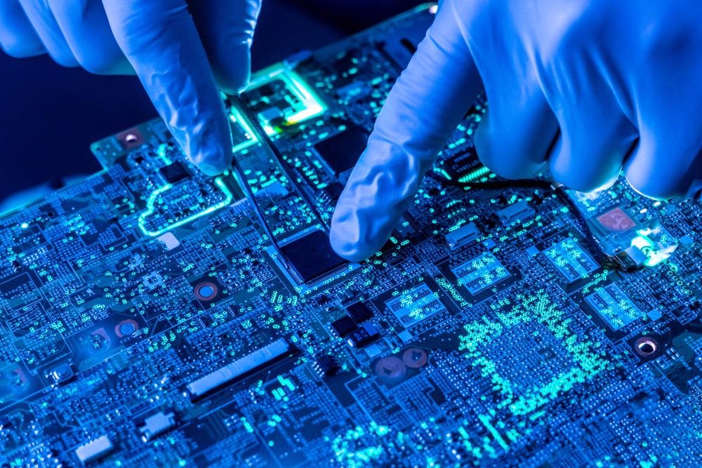
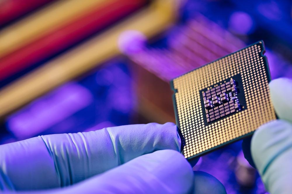
This article focuses on semiconductor fabrications steps, the photolithography process, and recent advances in this particular field.

Image Credit: Mike_shots/Shutterstock.com
Importance of Semiconductors
The ability to create materials with well-defined characteristics at the micro-and sub-micrometer dimensions is critical in a broad range of research fields and enterprises, from microelectronic chips and devices to tissue development. Since the 1970s, the semiconductor industry has spearheaded the creation of spatially designed materials with submicron precision, setting the trend toward generating increasingly complicated structured films and miniaturized electronics necessary in current digitalization.
Semiconductors can be found in laptops, consumer electronics, telecommunications equipment, industrial gear, automotive components, and military assets. Semiconductor materials in these goods perform services such as cognitive processing, visualization, energy control, storage systems, circuit design, and transformation between visual and electrical power sources.
Semiconductor Manufacturing Processes
The semiconductor and microchip fabrication process consists of several unique processing phases that result in a range of activities that may take place at a specific facility or in differing procedures at numerous facilities. Typical microchip production processes contain hundreds of stages, many of which are performed numerous times during the fabrication process. On the wafer, a large number of microscopic transistors are generated through a combination of physicochemical processes.
More from AZoM: The Role of Thin Oxide Films in Semiconductors
A few basic fabrication processes include deposition, oxidation, photolithography, doping, thin film deposition, etching, metallization, chemical mechanical planarization (CMP), and packaging.
Brief Explanation of Steps
The procedure starts with a silicon wafer substrate. Wafers are cut from a bar of 99.99 percent pure silicon (ingot) and refined to perfection. To provide a protective layer or shielding, silicon dioxide is produced or coated on the wafer. After that, the wafer is coated with a light-sensitive coating known as 'photoresist’.
Positive and negative resist are the two forms of resist. Lithography is an important phase since it sets the size of the transistors on a chip. The chip wafer is put into a lithography machine and subjected to deep ultraviolet (DUV) or intense ultraviolet (EUV) light at this step. Undesired sections of silicon framework substrate or coated film are eliminated to reveal a fundamental substance or to enable the alternative substance to be coated instead of the etched layer.
The conducting regions of the microchip are formed by depositing conductive metal onto the wafer. Finally, the surplus substance is eliminated from the wafer's bottom to ensure that the result has a smooth, smooth texture.
What is Photolithography?
The method of transmitting geometric forms to the base of a silicon wafer is known as photolithography. A light-sensitive photoresist is deposited on the wafer through a spin coating method. A photoresist solution of 1.5 to 5 mL is poured onto a wafer rotating at fast speed on a pressure clamp, allowing the photoresist to cover the semiconductor surface evenly.

Image Credit: mpohodzhay/Shutterstock.com
After spin coating, the wafer is "soft-baked" to remove the majority of the solvent from the photoresist. The resist's solid elements stay on the substrate surface and are then exposed to the air. Only in the portions of the substrate surface that are exposed to the environment does the photosensitive conduct a chemical reaction. The uncovered wafer is then "hard-baked" after a little time to improve resist adherence and prepare the surface layer for postprocessing.
Extreme ultraviolet lithography, or EUV lithography, is used in steppers, which are machines that make integrated circuits for computers and other electronic devices. EUV lithography machines can pattern fine details on advanced microchips.
Lithography Machines and Systems
Microchip lithography devices require three fundamental techniques, and their performance is determined by them. The first innovation is "the projection lens's resolution capabilities." The more complicated a circuit design that can be optically conveyed, the higher the resolution capability of the lens.
"Alignment accuracy" is the second technique. Photomasks must be changed tens of times and circuit designs must be carved continuously during the exposure process to manufacture a single transistor. As a result, the silicon wafer and photomask must be always perfectly coordinated. The third critical factor is "throughput." When transistors are mass-produced, this technology is critical. Throughput is a measure of efficiency that is stated as the number of silicon wafers exposed per hour.
Latest Research
A novel method has been proposed by researchers in an article published in the journal Analytical and Bioanalytical Biochemistry to develop and fabricate semiconductor electrophoresis devices with cross-shaped pathways and helical electrodes surrounding the detachment stream for microchip electrophoresis and capacitor-linked sensitive conductivity detection.
The whole gadget was created in poly(ethylene glycol) diacrylate polymer using a digital signal processing–based 3D printer. The 3D printing of microfluidic systems with 40 μm channels using DLP has been successfully proposed for MCE evaluation of reactive nitrogen species in biological materials. These microscopic gadgets might be used in ion analysis. By raising the operating speed, the voltage output grew until it reached its maximum value, after which it fell.
This was attributed to the detecting cell's capacitors: at a lower frequency, the wall channel capacitor predominated and absorbed most of the excitation source, whereas, at high frequencies, stray capacitances provided alternate signal routes. Even though the terminals were manufactured with the same material, the electrode helical geometry demonstrated here provided a greater linear response than the layout of the in-plane electrodes. This increase in linear response efficiency is anticipated for electrodes that approximate a tubular electrode.
In short, the lithographic techniques and systems have evolved ever since the dawn of the process, and research is focused on making it sustainable and emission-free.
References and Further Reading
ASML, 2022. 6 Crucial steps in semiconductor manufacturing. [Online]
Available at: https://www.asml.com/en/news/stories/2021/semiconductor-manufacturing-process-steps
Nikon, 2022. Semiconductor Lithography Systems. [Online]
Available at: https://www.nikon.com/about/technology/product/semiconductor/index.htm#:
Costa, B. et. al. 2022. 3D-printed microchip electrophoresis device containing spiral electrodes for integrated capacitively coupled contactless conductivity detection. Analytical and Bioanalytical Chemistry. 414(1). 545-550. Available at: https://link.springer.com/article/10.1007/s00216-021-03494-2
Costa, B. et. al. 2021. Microchip electrophoresis and electrochemical detection: A review on a growing synergistic implementation. Electrochimica Acta, 391, 138928. Available at: https://www.sciencedirect.com/science/article/pii/S0013468621012184?via%3Dihub
Shim, Hyunseok, Seonmin Jang, and Cunjiang Yu. 2022. High-resolution patterning of organic semiconductors toward industrialization of flexible organic electronics. Matter. 5(1) 23-25. Available at: https://www.sciencedirect.com/science/article/abs/pii/S2590238521005774
Disclaimer: The views expressed here are those of the author expressed in their private capacity and do not necessarily represent the views of AZoM.com Limited T/A AZoNetwork the owner and operator of this website. This disclaimer forms part of the Terms and conditions of use of this website.