A transparent conductive oxide (TCO) is a material that is optically transparent and electrically conductive. It is frequently utilized as a top electrode in thin-film solar cells, flat-panel displays (FPDs), and touch screens. Zinc oxide (ZnO) shows great promise in its utilization as a TCO.

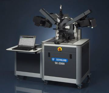
Figure 1. SE-2000. Image Credit: Semilab Semiconductor Physics Laboratory
The SE-2000 instrument from Semilab is a combined ellipsometry metrology system that has unique measurement abilities, ranging from mid-IR to UV.
This instrument is a strong candidate for industrial-scale metrology solutions to calculate layer thickness, as well as the electrical and optical properties of TCO layers in a non-destructive manner.
Spectroscopic Ellipsometry for Transparent Conductive Oxides Characterization
Metrology
This article presents a study using the spectroscopic ellipsometer with a wavelength range from 250 nm to 16 μm.
The layer thicknesses and the optical dispersion of the layer materials were established by modeling the layer structure and subsequently fitting the model parameters to match the simulated spectra to the measured ones.

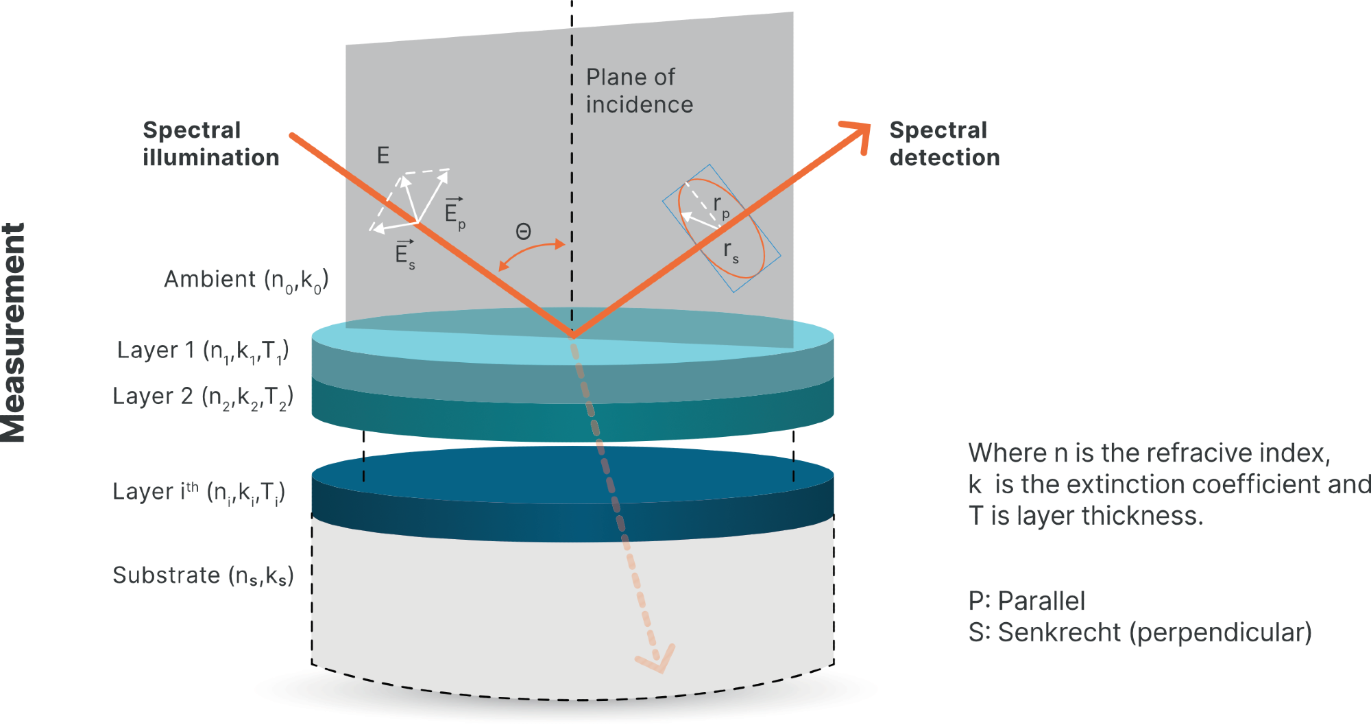
Figure 2. Schematic view of ellipsometry principle. Image Credit: Semilab Semiconductor Physics Laboratory
Use Case
Measurement example on atomic layer deposited, aluminum (Al) doped ZnO (AZO) layers. The addition of Al mainly increases the conductivity of n-type ZnO.

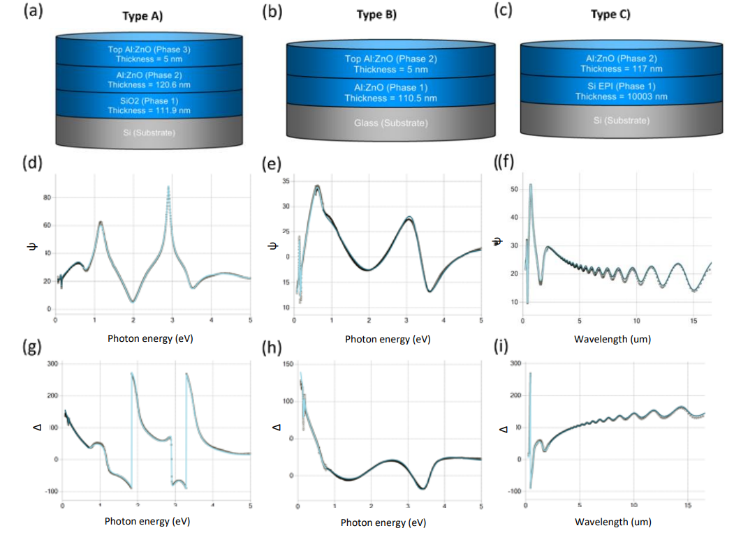
Figure 3. Model structures of the three different sample types: A) AZO layer on a Si substrate, 2.5% Al, 250 °C, B) AZO layer on a glass substrate, 3% Al, 225 °C, C) AZO layer on a Si-EPI on Si substrate, 3% Al, 225 °C. Image Credit: Semilab Semiconductor Physics Laboratory
Investigation of Atomic Layer Deposited Al:ZnO Layer
The multilayer structures demonstrate the model’s robustness and the need for the vast wavelength range measurements, particularly in the type C group where there is a Si EPI layer between the AZO layer and the substrate.
The ellipsometry model was able to differentiate the Si EPI from the AZO layer, as well as the substrate from the Si EPI layer on the AZO/Si-EPI/Si substrate sample type.
However, electrical measurements such as 4PP cannot separate the layers due to sheet resistance measurements combining the electrical properties of the entire stack.
Figure 4a-c shows that the highest dopant concentration can be obtained utilizing approximately 260 °C deposition temperature and approximately 2.5% target Al concentration.
Figure 4d presents the correlation of the two datasets (SE & 4PP), which displays a high correlation coefficient of 0.9993.
![Dopant concentration color maps as a function of process temperature and target Al concentration [(a)–(c)] and sheet resistance correlation plot between values obtained from ellipsometry characterization and 4PP measurements was selected for validation for AZO/glass type samples](https://www.azom.com/images/Article_Images/ImageForArticle_22836_16899329665811631.png)
Figure 4. Dopant concentration color maps as a function of process temperature and target Al concentration [(a)–(c)] and sheet resistance correlation plot between values obtained from ellipsometry characterization and 4PP measurements were selected for validation for AZO/glass type samples. Image Credit: Semilab Semiconductor Physics Laboratory
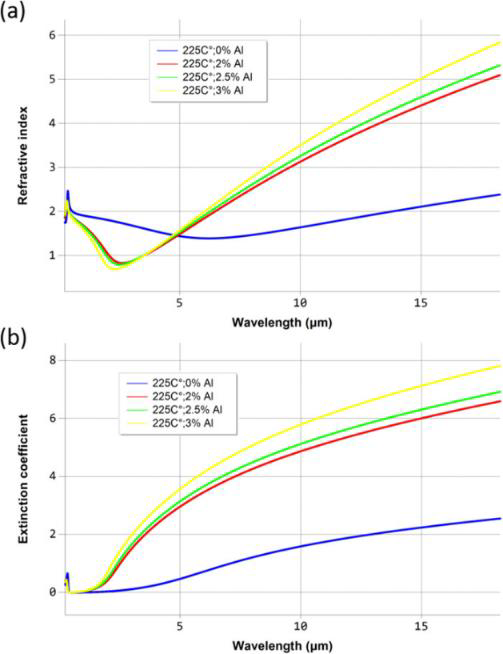
The parametric fits on the sample set measurements offer dispersion data that demonstrates sensitivity to the change in process parameters. Sensitivity to the Al% is apparent.

Figure 5. Refractive index (a) and extinction coefficient (b) of AZO of the type A samples for the 225 °C process temperature. Sensitivity to the Al% is apparent. Image Credit: Semilab Semiconductor Physics Laboratory
Materials and Structures
The above method could be also applied for other TCO materials, such as Indium Zinc Oxide (IZO), Indium Gallium Zinc Oxide (IGZO), AZO, etc., deposited on Si or glass substrate.
References
- László Makai et al., “Breakthrough instruments and products: Investigation of atomic layer deposited Al:ZnO layer by spectroscopic ellipsometry from the deep-UV to the mid-IR in one instrument” in AIP Publishing Volume 92, Issue 11, November 2021, doi: 10.1063/5.0071638.
- Anderson Janotti et al., "Fundamentals of zinc oxide as a semiconductor" in IOPscience, 22 October 2009, doi: 10.1088/0034-4885/72/12/126501

This information has been sourced, reviewed and adapted from materials provided by Semilab Semiconductor Physics Laboratory.
For more information on this source, please visit Semilab Semiconductor Physics Laboratory.