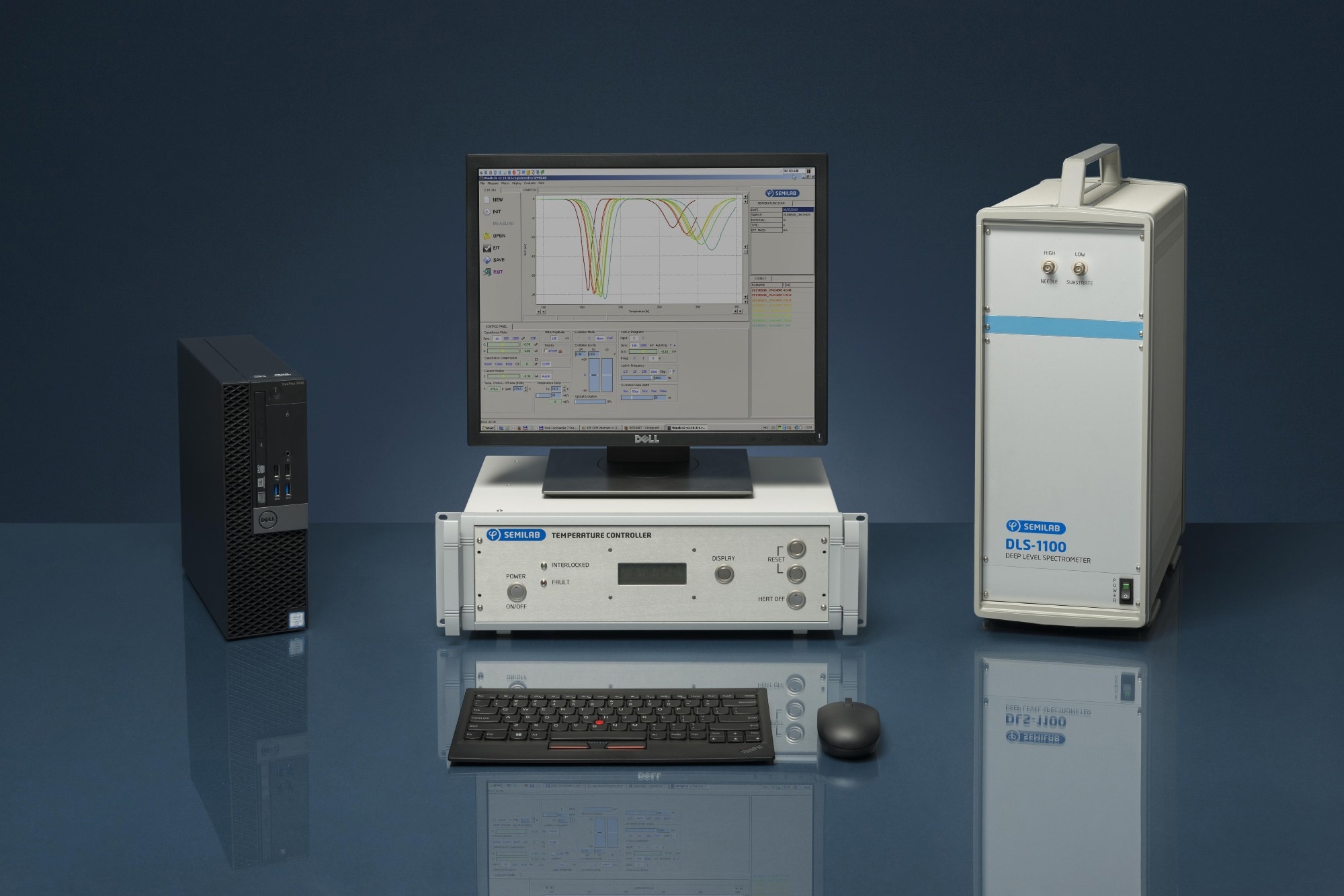
The Deep Level Transient Spectroscopy system gauges capacitance and current transients through a lock-in integrator and cryostat within the DLS system. Measurement modes encompass:
- Temperature/frequency scan
- Depth profiling
- CV characterization
- Capture cross-section
- Optical injection
- Transient digitization
Application Areas
- Wafer & EPI manufacturers
- IC fabs
- Research institutes

Figure 1. DLS system. Image Credit: Semilab Semiconductor Physics Laboratory
Metrology
The sample generates the capacitance transient, which is then measured by the instrument. A temperature sweep is applied while employing a lock-in technique. Subsequently, the instrument filters out noise and evaluates the transient signals.

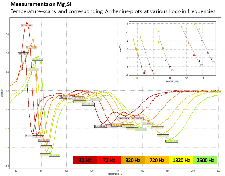
Figure 2. Measurements on Mg2Si temperature scans and corresponding Arrhenius plots at various Lock-in frequencies. The trend of a peak shift against the acquisition parameters makes it possible to deduce the activation energy and capture a cross-section of the related trap state. Image Credit: Semilab Semiconductor Physics Laboratory
- Acquiring the transient data provides the customer with accurate information about contamination and defects.
- Exceptionally high sensitivity, capable of detecting impurities below 2*108 atoms/cm3, is achieved due to the outstanding signal-to-noise ratio of the main measurement unit.
- Limitations: Destructive measurement necessitating sample preparation. Sample size depends on the cryostat, whose temperature range hinges on the specific application.
Use Case
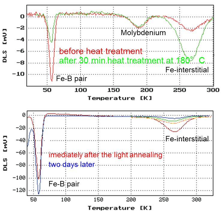
Fe contamination in Si is depicted in the figures below. Employing heat treatment, the Fe-B pair can be separated, resulting in an augmented Feinterstitial peak. This process is reversible; allowing the sample to relax reduces the peak once again.

Figure 3. Iron contamination in Silicon. Image Credit: Semilab Semiconductor Physics Laboratory
Materials and Structures
The characteristics of the ideal sample depend on the measurement's goal, with the following general conditions applying:
- The sample size falls within the 3x3 to 10x10 mm2 range with Schottky contact or an asymmetrical p-n junction.
- The depletion region does not surpass the layer thickness.
- Contact dimensions exceed 0.5x0.5 mm2.
The substrate boasts an ohmic contact with low resistivity.
Related Metrologies
- Surface PhotoVoltage (SPV)
- Microwave Photoconductance Decay (µ-PCD)
- Raman Spectroscopy
- Spectral Photoluminescence

This information has been sourced, reviewed and adapted from materials provided by Semilab Semiconductor Physics Laboratory.
For more information on this source, please visit Semilab Semiconductor Physics Laboratory.