Perovskite solar cells offer significant power conversion efficiencies and are relatively cost-effective to manufacture when compared to traditional silicon-based solar cells. Ideal perovskite layers exhibit substantial charge carrier mobility and a lengthy charge carrier diffusion length.
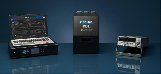
The tabletop Semilab PDL tool provides both AC and DC magnetic field Hall measurement methods with permanent magnets, integrated instrumentation, and software designed to boost research productivity.

Figure 1. PDL-1000 system. Image Credit: Semilab Semiconductor Physics Laboratory
Metrology
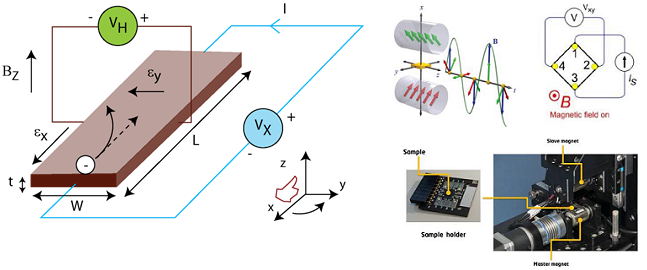
When a free charge carrier encounters an external electric field, it moves in the direction dictated by the field. Similarly, a charge carrier’s movement in the presence of a perpendicular magnetic field results in a force, as described by the Lorentz law, which alters its trajectory.
These phenomena lead to an uneven distribution of charge carriers within the measured sample.

Figure 2. Working principles of Hall measurement. Image Credit: Semilab Semiconductor Physics Laboratory
The Semilab PDL Hall technique measures the electrical potential between two sample points while current flows through the material between two other points, employing either the Van der Pauw or Hall bar geometry.
During the measurement process, two magnets rotate, generating a sinusoidal magnetic field that is perpendicular to the sample's surface. The reason for employing rotating magnets is to significantly improve the signal-to-noise ratio in the detection process. When the magnets rotate at a specific frequency, say, 1 revolution per minute (1 rpm), the resulting signal is inherently synchronized with this frequency. This synchronization makes it much easier to distinguish the signal of interest from any background noise or interference, ensuring that the measured data is highly accurate and reliable. This technique facilitates the determination of several key properties of the semiconductor, including its carrier type, charge carrier density, sheet resistance, and mobility.
Use Case
The mobility, charge carrier concentration, and resistance of the CH3NH3PbI3 perovskite sample under illumination were assessed using Semilab PDL Hall Measurement equipment.
Extracted parameters:
-
Carrier Type: n-type
- Sheet Carrier Density: -1.8 e + 07 cm-2
- Mobility: 3.09 cm2/Vs
- Sheet Resistance: 1.1+11 Ohm/sq.

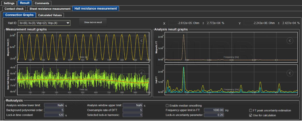
Figure 3. Window of PDL software with measurement and analysis result graphs. Image Credit: Semilab Semiconductor Physics Laboratory
On figure 3, the top left figure displays the measurement of the magnetic field, showing continuous sinusoidal curve. This curve represents the magnetic field's strength over time.
In the lower left figure, you can observe the Hall voltage and its correlation with changes in the magnetic field. As per the Hall effect, when a current flows through a conducting material in the presence of a perpendicular magnetic field, it creates a voltage across the material. The Hall voltage is a critical parameter for understanding the electrical properties of the material being tested.
The right-hand panel presents the Fourier transform of the two signals mentioned earlier. The Fourier transform is a mathematical technique used to analyze the frequency components of a signal. In this context, it helps in identifying and quantifying the specific frequency at which the magnet rotates.
Materials and Structures
Perovskite materials follow the ABX3 formula, where A denotes an organic/inorganic cation, B stands for a metal cation, and X represents an anion.
Measurements of photovoltaic, thermoelectric or semiconductor materials with mobilities as low as 0.01 cm2/Vs (and typically below 0.1 cm2/Vs) are achievable with the PDL-1000.
Related publications about dark Hall and CRPH measurements and results
- Julie Euvrard et al., “Impact of PbI2 Passivation and Grain Size Engineering in CH3NH3PbI3 Solar Absorbers as Revealed by Carrier-Resolved Photo-Hall Technique” in Advanced Energy Materials, Nov 2019, doi: 10.1002/aenm.201902706
- Julie Euvrard et al., “p-Type molecular doping by charge transfer in halide perovskite” in Materials Advances, 2021, doi: 10.1039/d1ma00160d
Related Metrologies
- Automated mobility mapping (MBM)
- 4-point probe (4PP)

This information has been sourced, reviewed and adapted from materials provided by Semilab Semiconductor Physics Laboratory.
For more information on this source, please visit Semilab Semiconductor Physics Laboratory.