 By JanakyReviewed by Lexie CornerSep 6 2024
Optoelectronics, a sub-discipline of photonics, involves the study and application of devices that emit, detect, or control light.1 Optoelectronic Materials (OEM) are a specific class of semiconductor materials that facilitate the conversion between light and electricity (photons and electrons).
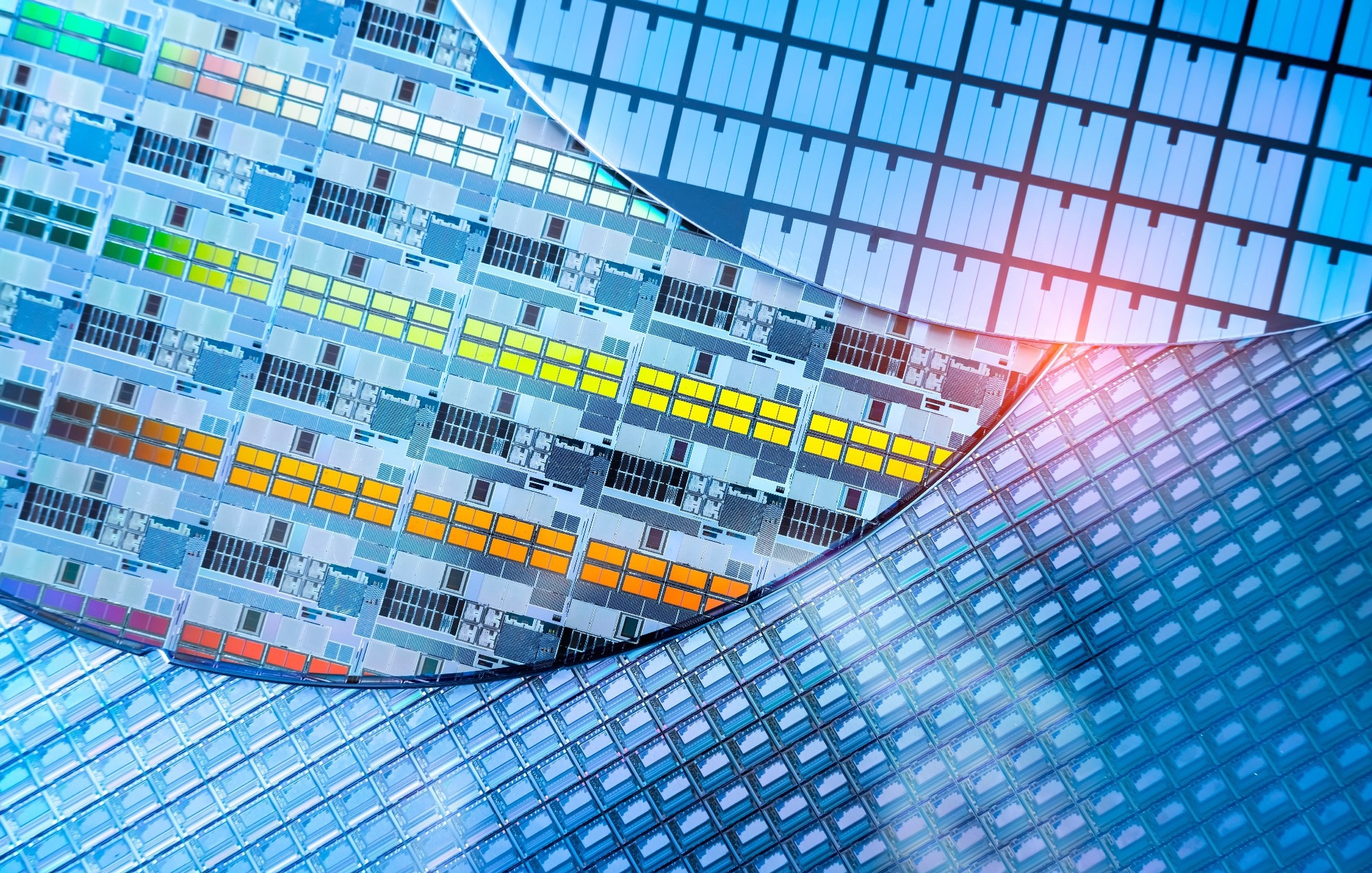
Image Credit: asharkyu/Shutterstock.com
They are essential to a wide range of devices, from LEDs and solar panels to modern technologies like thin-film transistors and quantum information systems.2
OEM Interactions with Light and Electricity
Optoelectronic materials convert light into electricity and vice versa. When light strikes an OEM, its energy is absorbed by electrons in the crystal lattice. The electrons that absorb this energy jump from the low-energy valence band to the high-energy conduction band, crossing the energy gap.1
If the photon's energy exceeds the bandgap, the electron may leave the material, resulting in effects such as increased electrical conductivity (photoconductivity) or the emission of electrons (photoelectric effect).3
This principle also allows light generation from electrical signals. Photon emission occurs when an excited electron returns to a lower energy state, as seen in devices like LEDs and lasers.1 The wavelengths of light absorbed or emitted by OEMs and their optical properties depend largely on the material’s bandgap.
Common Types of OEM
Semiconductors are the most common OEMs, known for their ability to control electrical conductivity.
Silicon, the most widely used, is favored for its abundance, affordability, and optical properties like a high refractive index.4 Doping silicon introduces impurities that create either n-type or p-type semiconductors, with n-type having more electrons and p-type having more holes.
While both types can function as OEMs, most two-dimensional semiconductors are typically n-type due to the presence of strong electron-doping impurities and structural defects at their interfaces.
Photodetectors are a well-known category of OEMs, with common examples including photodiodes based on p-n junctions and photovoltaic (PV) cells, which often use silicon. III–V compound semiconductors like GaN and GaAs offer advantages such as high absorption efficiency, fast carrier drift velocity, and well-established technology for designing and manufacturing optical devices.5
Metal oxides, known for their high carrier mobility even in an amorphous state, also offer strong mechanical stress tolerance, making them well-suited for photoelectric applications.6
Organic light-emitting diodes (OLEDs), made from lightweight and flexible organic compounds, represent a distinct category of OEMs. These materials emit light, with the wavelength determined by their bandgap, when an electric current passes through them, making them highly effective light sources.7
Besides their flexibility, these organic thin-film semiconductor devices are known for their ultra-thin profiles, nominal energy expense, and potential for large-area processing. OLEDs are particularly valued for their ability to produce bright, vibrant displays while maintaining low power usage.7
Quantum dots, with their tunable bandgap for detecting specific wavelengths, are emerging as highly sensitive photodetectors.8 Their discrete energy levels and enhanced quantum efficiency make them ideal for applications requiring high-resolution light detection.8 As the field evolves, new synthetic approaches are enabling precise molecular design, allowing for materials with tailored properties.
Applications of OEM in Advanced Devices
Optoelectronics encompasses a wide range of devices, including telecommunication lasers, optical fibers, blue lasers, LEDs, photodiodes, and solar cells.2 OEMs are integral to these technologies, as they harness the interaction between light and electricity.
In telecommunications, the ability to transmit data over optical fibers has underpinned the development of global internet infrastructure, enabling the high-speed connectivity that powers modern communication networks.
LEDs, which emit light when electrons recombine with holes, are common in lighting, displays, and indicators.1 LEDs have revolutionized everyday life, from large-scale displays to household lighting, thanks to their energy efficiency and long lifespans.
OLEDs, another key advancement, allow for the creation of thinner, flexible, and more vibrant screens. These screens are now widely used in smartphones, televisions, and wearable devices.7
OEMs are also crucial in the energy sector, serving as the foundational technology behind solar cells, which convert sunlight into electrical energy.2 Ongoing research focuses on next-generation thin-film photovoltaic (PV) devices, exploring cost-effective and eco-friendly alternatives to silicon that offer superior light absorption for enhanced solar energy conversion.
The photovoltaic effect, which generates electron-hole pairs when exposed to light, is harnessed in devices such as photodiodes, solar cells, phototransistors, and opto-isolators.1
OEMs also exhibit photoconductivity, enabling various forms of light detection and imaging in devices like photoresistors, photoconductive camera tubes, and charge-coupled imaging devices.1 Additionally, the emissivity of certain OEMs is applied in photoemissive camera tubes used for specialized imaging technologies.
Another fundamental process, stimulated emission, is the basis for technologies like laser diodes, injection laser diodes, and quantum cascade lasers. These devices amplify light by stimulated emission, generating coherent light essential for applications in communication systems, barcode scanners, optical disc drives, and high-precision measurements.9
Beyond communication and energy, OEMs are increasingly being used in military and aerospace technologies, medical equipment, and automated systems.
Advancements in OEMs for Modern Technological Applications
Advancements in semiconductor growth techniques, such as molecular-beam epitaxy and vapor-phase epitaxy, have been instrumental in developing two-dimensional OEMs for novel applications.11
Ongoing research into new semiconductor materials, like perovskites and organic photovoltaics, aims to enhance the efficiency, cost-effectiveness, and flexibility of solar cells.12
The development of nanoscale structures, such as quantum dots and quantum wells, has also shown great potential to boost efficiency by reducing energy losses and enabling multi-junction configurations, which absorb different wavelengths of light more effectively.8
These advancements are driven by the ability to engineer materials at the molecular level, optimizing their properties to capture a broader spectrum of sunlight. As research in this area continues, the potential for these materials to drive future innovations remains vast, solidifying their role as a cornerstone of the technologies that shape our daily lives.2
These innovations promise more efficient, cost-effective, and sustainable manufacturing processes, ensuring that optoelectronic materials will remain crucial in advancing technological progress.
More from AZoM: Comparing Particle Counters in a Semiconductor Cleanroom Environment
References and Further Reading
- TT Electronics. (2022). Optoelectronics: Emerging Technology Focused on Light-Detecting Devices. [Online] TT Electronics. Available at: https://www.ttelectronics.com/blog/optoelectronics
- Vashisht, M. (2022), Optoelectronics and its Omniscient Array of Industrial Application. [Online] ELETimes. Available at: https://www.eletimes.com/optoelectronics-and-its-omniscient-array-of-industrial-application
- Silvestre, S. (2017), Optoelectronics, photonics and sensors. [Online]. Techpedia. ISBN: 978-80-01-06262-3. Available at: https://psm.fei.stuba.sk/pages/125/LM14_F_EN.pdf
- Gao, D., Zhou, Z. (2022). Silicon-based optoelectronics: progress towards large scale optoelectronic integration and applications. Frontiers of Optoelectronics. DOI: 10.1007/s12200-022-00030-7, https://link.springer.com/article/10.1007/s12200-022-00030-7
- Zhao, C., et al., (2018). III-nitride nanowires on unconventional substrates: From materials to optoelectronic device applications. Progress in Quantum Electronics. DOI: 10.1016/j.pquantelec.2018.07.001, https://www.sciencedirect.com/science/article/pii/S0079672718300302
- Yu, X., Marks, TJ., Facchetti, A. (2016). Metal oxides for optoelectronic applications. Nature materials. DOI: 10.1038/nmat4599, https://www.nature.com/articles/nmat4599
- Shirota, Y., Kageyama, H. (2019). Organic materials for optoelectronic applications: Overview. Handbook of Organic Materials for Electronic and Photonic Devices. DOI: 10.1016/B978-0-08-102284-9.00001-2, https://www.sciencedirect.com/science/article/abs/pii/B9780081022849000012
- Wu, J., Chen, S., Seeds, A., Liu, H. (2015). Quantum dot optoelectronic devices: lasers, photodetectors and solar cells. Journal of Physics D: Applied Physics. DOI: 10.1088/0022-3727/48/36/363001, https://iopscience.iop.org/article/10.1088/0022-3727/48/36/363001/meta
- Vitiello, MS., Tredicucci, A. (2021). Physics and technology of Terahertz quantum cascade lasers. Advances in Physics: X. DOI: 10.1080/23746149.2021.1893809, https://www.tandfonline.com/doi/full/10.1080/23746149.2021.1893809
- Rogalski, A., Chrzanowski, K. (2017). Infrared devices and techniques. In Handbook of optoelectronics, CRC Press. pp.633-686. ISBN: 9781315157009, https://www.taylorfrancis.com/chapters/edit/10.1201/9781315157009-18
- Zhao, C., et al., (2021). Novel III-V semiconductor epitaxy for optoelectronic devices through two-dimensional materials. Progress in Quantum Electronics. DOI: 10.1016/j.pquantelec.2020.100313, https://www.sciencedirect.com/science/article/abs/pii/S0079672720300720
- Machín, A., Márquez, F. (2024). Advancements in photovoltaic cell materials: Silicon, Organic, and Perovskite Solar cells. Materials. DOI: 10.3390/ma17051165, https://www.mdpi.com/1996-1944/17/5/1165
Disclaimer: The views expressed here are those of the author expressed in their private capacity and do not necessarily represent the views of AZoM.com Limited T/A AZoNetwork the owner and operator of this website. This disclaimer forms part of the Terms and conditions of use of this website.