Originating as a theoretical prediction in the 1940s, with experimental isolation from graphite in 2004, graphene has quickly become a desirable quantum material used in various application areas, such as semiconductors, microelectronics, bioengineering, composites, and batteries.1,2 The production of defect-free, large-scale, layer-uniform graphene devices is critical in many situations. Pristine monolayer graphene has exceptional thermal, mechanical, and electronic properties that shift with rising layer numbers, strain, and defects.3 Therefore, methods to probe uniformity across graphene devices are essential for quality assurance.
The Edinburgh Instruments RM5 Confocal Raman Microscope is ideally suited for analyzing graphene. Raman mapping can reveal details on the structural and electronic properties of graphene and map the location of structural defects, doping, strain, and layer stacking through the relative intensity and positioning of the Raman bands in the graphene spectrum.
This article demonstrates the capability of the RM5 and Ramacle® software for graphene analysis by mapping the layer number, defects, and strain on graphene films.
Materials and Methods
The samples used in the analysis were monolayer and bilayer graphene films deposited on Si substrates. The Raman mapping was completed with an Edinburgh Instruments RM5 equipped with a 532 nm laser, a 100X 0.9 NA objective, and a CCD detector (Figure 1). The mapping data was analyzed and plotted using the RM5’s Ramacle software package.
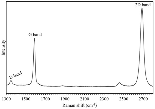
Figure 1. Raman spectrum of graphene with the common modes used for mapping labeled. Image Credit: Edinburgh Instruments
Raman Spectrum of Graphene
Graphene’s Raman spectrum and the key bands used for mapping are seen in Figure 2. The D band ca. 1350 cm-1 is a ring breathing mode of the sp2 carbon ring and is Raman active in defective graphene. The G band ca. 1585 cm-1 is the result of an in-plane stretching vibrational mode of the sp2 bonds, and the 2D band ca. 2680 cm-1 comes from a double resonance enhanced two-phonon lateral vibrational process.4
Figure 2. Edinburgh Instruments RM5 Raman Microscope. Image Credit: Edinburgh Instruments
Layer Number: Ratiometric Mapping of G and 2D Bands
The differences in layer number throughout the graphene sample can be determined using the relative peak intensities of the G band (IG) and the 2D band (I2D) in the Raman spectrum.5 As the number of layers in graphene rises, IG increases relative to I2D.6 Therefore, the 2D/G band ratio (I2D/IG) can map the uniformity and layer number across graphene films and flakes.
The RM5 mapped a nominally bilayer graphene sample. Maps of IG, I2D, and the peak ratio I2D/IG were plotted in Ramacle, as seen in Figure 3.
The I2D/IG peak ratio is significantly variable over the map between 0.1 and 2 (Figure 3c), indicative of a notable variance in layer numbers across the sample.
Monolayer graphene is commonly characterized by an I2D/IG of ≥ 2, while in bilayer graphene, I2D/IG is near 1. A greater number of graphene layers cause I2D/IG values to be less than 1.7,8 As a result, the black areas (high I2D/IG) on the map were assigned as monolayer graphene, the purple as bilayer, and the yellow (low I2D/IG) as multilayer. The spectra in Figure 3d demonstrate the significant change in I2D/IG in the spectra collected from these different regions.
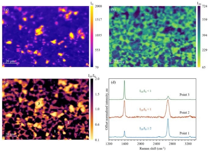
Figure 3. I2D/IG Raman mapping of graphene for layer number determination. Image Credit: Edinburgh Instruments
Strain: Peak Position Mapping of G and 2D Bands
Material strain changes bond lengths, which alters their vibrational frequencies and the properties of the material being investigated.
Raman spectroscopy is particularly sensitive to strain. With graphene, strain is related to frequency changes in the vibrational modes. This is mirrored in the Raman shift of the G and 2D bands, allowing the position of these bands to create a strain map of the graphene surface.7
A monolayer film grown on a Si wafer containing numerous fissures was mapped to track strain in graphene through Raman microscopy (Figure 4). The region mapped on the sample contained two fissures in the Si substrate, which were hypothetically thought to affect the mechanical properties of the graphene film layered on top and instigate strain. A peak position image for the G band was created (Figure 4b), demonstrating a lowered band frequency in the areas where the graphene lay over the fissures.
The G band frequency reduction can be attributed to tensile stress in the graphene layer. Tensile stress elongates the graphene sheet, lowering the vibrational mode energies and wavenumbers. Spectra from both unstrained and strained areas are depicted in Figure 4c, which also shows that the frequency of the 2D band reduces in the strained graphene.
The decrease in frequency of the G band in Figure 4b might also result from raising graphene layer numbers. However, IG would increase as layer numbers increase, and Figure 4a demonstrates that regions with a decrease in G band frequency also have a reduced IG. This means it is possible to conclude that the peak shifts are caused by strain rather than layer number. The intensity map also highlighted areas of high IG, shaded in cream, which could be assigned as multilayer graphene.
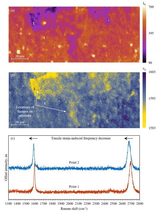
Figure 4. Peak position Raman mapping of graphene for strain detection. Image Credit: Edinburgh Instruments
Defects: Ratiometric Mapping of D and G Bands
Raman microscopy can track defects on graphene samples due to the disorder in the lattice creating D and D’ Raman peaks ca. 1350 cm-1 and 1640 cm-1, which are otherwise Raman-forbidden.
These are allowed in spectra of defective graphene as the defect provides the missing momentum to satisfy conservation in the Raman scattering process.8 The amount and characteristics of the graphene defects can significantly affect the performance, either in detrimental or advantageous ways, depending on the intended material application. For example, defects have previously diminished electron mobility on graphene deposited on substrates but have also enhanced the reactivity of graphene-based catalysts.9,10
The graphene sample was mapped on the RM5, ID, and IG, and plotted in Ramacle, Figure 5a and b. ID/IG was then plotted in Ramacle, and the resulting image is seen in Figure 5c.
ID/IG is a worthwhile metric for determining pristine and defect-dense graphene areas. When the graphene is pristine, the ratio is often close to 0. As the defect density increases, the ratio will rise.
In Figure 5c, the dark blue regions are low-defect-density graphene, while the red and yellow areas are high-defect-density graphene. Spectra from a range of map regions are shown in Figure 5d.
In the high-defect-density region, the D band shows more intensity than the G band, comparable to the low-defect-density region where the G band is dominant, and no D band is seen.
The D' band is present in the defect-dense areas, appearing as a higher-Raman shift shoulder of the G band. The ratio between the D and D’ bands can be utilized to differentiate between defect types; for example, a greater value is attributed to sp3-type defects, and lower values are associated with vacancy-type defects.8
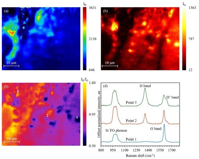
Figure 5. ID/IG Raman mapping of graphene for defect detection. Image Credit: Edinburgh Instruments
Conclusion
An Edinburgh Instruments RM5 Confocal Raman Microscope helped map graphene films' layer number, defect density, and strain.
The RM5 is ideally suited for graphene analysis, as it reveals a great deal of information regarding the structural and electronic properties of the graphene layer with high sensitivity and spatial resolution.
References and Further Reading
- Wallace, P.R. (1947). The Band Theory of Graphite. Physical Review, 71(9), pp.622–634. https://doi.org/10.1103/physrev.71.622.
- Novoselov, K.S. (2004). Electric Field Effect in Atomically Thin Carbon Films. Science, (online) 306(5696), pp.666–669. https://doi.org/10.1126/science.1102896.
- Asad, S., et al. (2022). Recent Advances in Titanium Carbide MXene (Ti3C2Tx) Cathode Material for Lithium–Air Battery. ACS Applied Energy Materials, 5(10), pp.11933–11946. https://doi.org/10.1021/acsaem.2c01845.
- enezuela, P., Lazzeri, M. and Mauri, F. (2011). Theory of double-resonant Raman spectra in graphene: Intensity and line shape of defect-induced and two-phonon bands. Physical Review B, 84(3). https://doi.org/10.1103/physrevb.84.035433.
- Yu, X., et al. (2018). Synthesis of transfer-free graphene on cemented carbide surface. Scientific Reports, 8(1). https://doi.org/10.1038/s41598-018-23206-8.
- Ferrari, A.C. (2007). Raman spectroscopy of graphene and graphite: Disorder, electron–phonon coupling, doping and nonadiabatic effects. Solid State Communications, (online) 143(1), pp.47–57. https://doi.org/10.1016/j.ssc.2007.03.052.
- Ni, Z.H., et al. (2008). Uniaxial Strain on Graphene: Raman Spectroscopy Study and Band-Gap Opening. ACS Nano, 2(11), pp.2301–2305. https://doi.org/10.1021/nn800459e.
- Eckmann, A., et al. (2012). Probing the Nature of Defects in Graphene by Raman Spectroscopy. Nano Letters, 12(8), pp.3925–3930. https://doi.org/10.1021/nl300901a.
- Ni, Z.H., et al. (2010). On Resonant Scatterers As a Factor Limiting Carrier Mobility in Graphene. Nano Letters, 10(10), pp.3868–3872. https://doi.org/10.1021/nl101399r.
- Boukhvalov, D.W. and Katsnelson, M.I. (2008). Chemical Functionalization of Graphene with Defects. Nano Letters, 8(12), pp.4373–4379. https://doi.org/10.1021/nl802234n.

This information has been sourced, reviewed and adapted from materials provided by Edinburgh Instruments.
For more information on this source, please visit Edinburgh Instruments.