Sep 17 2007
All researchers at the National Institute of Standards and Technology (NIST) wanted was a simple, quick method for making thin films of block copolymers or BCPs (chemically distinct polymers linked together) in order to have decent samples for taking measurements important to the microelectronics industry.
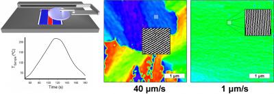 Caption: (Top L.) Schematic of the NIST 'cold zone' annealing process for polymer thin films on a semiconductor wafer. Experiment images are color-coded to show regions with different cylinder orientations, as measured by atomic force microscopy. Relatively rapid transit times (top r.) leave a jumble of different regions that become largely homogeneous at slower speeds (r.).
What they got for their efforts, as detailed in the Sept. 12, 2007, Nano Letters, was an unexpected bonus: a unique annealing process that may make practical the use of BCP thin films for patterning nanoscale features in next-generation microchips and data storage devices.
BCP thin films have been highly desired by semiconductor manufacturers as patterns for laying down very fine features on microchips, such as arrays of tightly spaced, nanoscale lines. Annealing certain BCP films—a controlled heating process—causes one of the two polymer components to segregate into regular patterns of nanocylinder lines separated by distances as small as five nanometers or equally regular arrays of nanoscale dots. Chemically removing the other polymer leaves the pattern behind as a template for building structures on the microchip.
In traditional oven annealing the quality of the films is still insufficient even after days of annealing. A process called hot zone annealing—where the thin film moves at an extremely slow speed through a heated region that temporarily raises its temperature to a point just above that at which the cylinders become disordered—has previously been used for creating highly ordered BCP thin films with a minimum of defects but little orientation control. For some polymer combinations, the order-disorder transition temperature is so high that it is virtually impossible for manufacturers to heat them sufficiently without degradation occurring.
To eliminate the time and temperature restraints without losing the order yielded by hot zone annealing, the NIST researchers developed a “cold zone” annealing system where the polymers are completely processed well below their order-disorder transition temperature. Properly controlled, the lower-temperature processing not only works with BCPs for which hot-zone annealing is impractical, but, as the NIST experiments showed, also repeatedly produces a highly ordered thin film in a matter of minutes. NIST researchers also discovered that the alignment of the cylinders was controlled by the “cold zone” annealing conditions. Because it is simple, yields consistent product quality and has virtually no limitations on sample dimensions, the NIST method is being evaluated by microelectronic companies to fabricate highly ordered sub 30 nm features.
The next step, the NIST researchers say, is to better understand the fundamental processes that make the cold zone annealing system work so well and refine the measurements needed to evaluate its performance.
http://www.nist.gov