Oct 23 2009
Researchers from the MESA+ Institute for Nanotechnology at the University of Twente, The Netherlands, working with American researchers, have succeeded in using an electrical signal to control both the elastic and the magnetic properties of a nanomaterial at a very localized level. This opens up new possibilities for data storage with very high data densities. Their findings are to be published in November in the leading scientific journal Nature Nanotechnology.
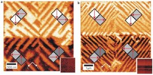
 Manipulation of the polarization in nanostructures. In Figure a, the researchers created an artificial star; in Figure b there is a diamond pattern.
In what are known as 'multiferroic' materials, the electrical, magnetic and elastic properties of the material are coupled. These materials make it possible to create new, complex structures that are suitable for e.g. data storage. Until recently, nobody had succeeded in controlling these multiferroic properties, but researchers from Oakridge National Laboratory, the University of California, Berkeley, Pennsylvania State University and the University of Twente's MESA+ Institute for Nanotechnology demonstrate in the next issue of Nature Nanotechnology that it is indeed possible.
In their experiments, the scientists succeeded in manipulating a nanostructure made of bismuth ferrate (BiFeO3) in an ordered way using scanning probe microscopy. This is a technique in which a surface can be manipulated at the atomic scale, using a miniscule needle.
By applying an electrical voltage to the needle and moving it over the surface of the material, the scientists are able to 'charge' a nanomaterial with different elastic and magnetic properties at a very localized level. This opens new avenues for data storage with very high information densities.
More information: The article 'Deterministic control of ferroelastic switching in multiferroic materials' by N. Balke, S. Jesse, A. P. Baddorf, S. V. Kalinin (ORNL), Y. H. Chu, R. Ramesh (UC Berkeley), S. Choudhury and L. Q. Chen (Penn State) and M. Huijben (MESA+) will appear in the November issue of Nature Nanotechnology.