Following the growing demand from the market LayTec now offers a new EpiTT version offering three simultaneous reflectance measurements. With EpiTT 3W now more complex in-situ growth studies of compound semiconductor devices composed of materials having rather wide band edges can be performed.
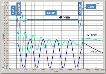
 Figure 1. a typical AlGaInP/GaInP double hetero-structure on
GaAs that Tobias typically grows for test purposes.
Tobias Roesener from ISE Freiburg was one of the first customers to use the EpiTT 3W. He is working on III-V growth on Silicon for future solar cell applications in a CRIUS MOCVD system.
Tobias stated: "The reflectance measurements at 633nm and 950nm have already been very helpful for us. Now with the addition of the 405nm reflectance measurement in my case I got far more sensitive access to the surface morphology. Particularly it allows me a much better monitoring of surface morphology evolution in thinner layers such as GaInP after only 50 to 100nm (see figure 1). The 633nm reflectance measurement is perfectly suited for GaInP growth control. At this wavelength we determine growth rates of layers which are below 100nm thick. The reflectance at 950nm is better suited for thicker layers." He added that for growth of Germanium layers, the application of the 950nm signal is extremely useful. For homo-epitaxial growth of Germanium under different growth conditions (temperature, pressure, gas flows) the growth rate and the decomposition of the source materials can be derived in-situ in one single epitaxial process. "This saves me a lot of development time!" he stated.
The EpiTT 3W is equipped with 405nmn, 633nm and 950nm reflectance as a standard and thereby is perfectly suited for all III-As/P and III-Nitride processes. The new 3W option is of course available for LayTec´s EpiCurve TT systems as well and all existing EpiTT, Twin TT and EpiCurve TT systems in the field can be up-graded on-site!
If you are interested in further information about EpiTT 3W please contact: [email protected].