It has become a good Laytec tradition: November, 29th and 30th 2011 for the 8th time LayTec held its private seminar in Tokyo and Nagoya, Japan.
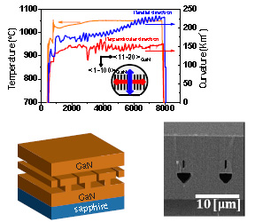
 In-situ curvature measurement in two different directions
(blue: parallel to GaN stripes, red: perpendicular to GaN stripes) and
temperature measurement during the growth of GaN on a striped
GaN/void structure.
New in-situ measurement approaches for multiple applications as well as product news were presented.
Prof. Sugiyama of University of Tokyo reported on successful strain compensation of InGaAs/GaAsP multiple quantum wells (MQWs) using both EpiRAS and EpiCurve TT for novel solar cell applications on GaAs. Interestingly, the H2-purging and subsequent As-/P-stabilization of the InGaAs surface directly influences the resulting bulk strain of MQW structures. He clarified that at least 3 seconds with only TBAs and TBP flow are necessary before TMGa gas flow restarts for GaAsP well growth. Only runs using this technique showed completely flat wafers after MQW growth.
Prof. Miyake of Mie University presented high crystal quality GaN on sapphire wafers by controlling overgrowth of stripe patterned GaN buffers including stripe-voids from former SiO2 masking. The overgrowth of this GaN stripe-void-structure with a GaN cap layer was optimized by precise control of the anisotropic, aspherical bow of the wafer using an EpiCurve TT metrology system.
Last but not least examples of curvature engineering for GaN on Si devices were presented by Dr. Yuto Tomita of LayTec AG.
All talks of the seminars in Tokyo and Nagoya are now available for download from the Laytec website! To obtain a log-in ID please contact [email protected].
Laytec would like to thank all the speakers for their excellent presentations and their partner Marubun for their great support.