Jun 30 2015
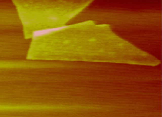
 Atomic force microscope image of a black arsenic-phosphorus field-effect transistor, image courtesy of Chongwu Zhou and Bilu Liu
This new method does not require high pressure and is cheaper and requires less energy. Customers had complained that the new iPhone could be bent. However, based on research conducted by engineers at USC Viterbi, large phones that could be rolled to fit the pocket could soon be a reality.
Silicon has played a critical role in modern electronics for many decades; however, it has limitations as the latest devices keep becoming smaller, requiring transistors that are tinier than before.
The silicon transistor is reaching the maximum smallest size that it can be manufactured. A top-down cutting method is used for silicon devices, and making smaller silicon is becoming more difficult. Furthermore, consumers are demanding phones that are faster, smaller, lighter, bendable, wearable and more flexible.
However, as silicon is rigid, it can’t be used in computers or smartphones that need to be bent. Hence, it has induced the industry to search for new alternative materials for silicon that can be used for semiconductor applications.
Graphene was discovered as a result of the demand for a silicon material. Graphene is made up of a single layer of graphite. In 2010, graphene’s discovery won the Nobel Prize. Following this discovery, many 2D material innovations have been developed.
2D materials are layered materials that have the thickness of a single atom or a couple of atoms. Black arsenic phosphorous is a 2D material, and the current study is about an innovative method for synthesizing black arsenic-phosphorous.
The black arsenic-phosphorous material demonstrates astounding properties that are not demonstrated by any other 2D material. This material has small energy gaps that allow it to sense long wavelength infrared (LWIR) waves. During synthesis of the material, its chemical compositions can also be manipulated.
In LIDAR (light radar) systems and similar applications, LWIR’s spectral range is very important, as they are highly transparent in the atmosphere. LWIR is also useful in flexible night vision glasses, and for infrared thermal imaging technology used by military soldiers.
This layered semiconductor material has unique anisotropic optical and electronic properties, which means that it even in the same plane, it has dissimilar properties along the x and y directions. When compared to existing materials, these properties hold more advantages, which could help develop unique applications, such as devices for environmental monitoring.
We believe these materials are important members in a large family of 2D materials, because they fit into the long-wavelength-infrared light range and deliver properties that any other currently existing 2D materials cannot.
Professor Chongwu Zhou, Ming Hsieh Department of Electrical Engineering
According to Bilu Liu, the paper’s lead author and postdoctoral researcher: “As these are rather new materials, we anticipate there is lots of exciting fundamental physics research as well as engineering work to be done. For example, what’s the electronic and optical properties of a truly single layer black arsenic phosphorus?”
This study has been published as a paper entitled 'Black Arsenic-Phosphorus: Layered Anisotropic Infrared Semiconductors with Highly Tunable Compositions and Properties' in the journal Advanced Materials.