The Fraunhofer Institute for Photonic Microsystems in Dresden, Germany has installed a FlexAL system for plasma enhanced and thermal ALD from Oxford Instruments Plasma Technology in its Center for Nanoelectronic Technologies.
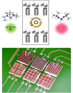
 (top to bottom) FhG IPMS-CNT’s FlexAL applications: ultra-thin integrated 3D capacitors, ALD/PEALD precursor development.
The fields of use for the new tool are research and development on processes for metal oxides for ultra-thin integrated 3D capacitors, the development of new and unique metal ALD processes, and as a platform with a combinatorial screening concept including in-situ metrology and standardised tests for ALD/PEALD precursor development serving gas and chemical supplying companies. Additionally the FlexAL will serve as a 200mm PEALD tool for the MOEMS pilot line at the Fraunhofer IPMS.
“The Center for Nanoelectronic Technologies has a long-term experience in atomic layer deposition (ALD), which is a sophisticated process where monolayer after monolayer is built up”, comments Dr. Romy Liske, Business Unit Manager of the FhG IPMS-CNT, “ALD is the process of choice whenever precise thickness and composition control of thin films in the nanometer range are required.
This is particularly the case for semiconductor devices where the smallest dimensions of some tens of nanometer are fabricated, and an increasing demand is observed for high conformal thin ALD films. Consequently, the development of materials and compounds deposited by ALD increases impressively.”
After a rigid tendering process the Oxford Instruments FlexAL PEALD system was chosen because of its capabilities as a high end ALD research and development tool. The broad range of processes enabled by the FlexAL’s design allows the combination of plasma and thermal processes in one fully automated recipe as well as the flexible precursor cabinet which enables effective combinatorial precursor screening with in-situ metrology.
“The proven performance and versatility of the Oxford Instruments FlexAL together with the availability of multiple room temperature variants of PEALD processes made it the ‘system of choice’ for the Center for Nanoelectronic Technologies. We are extremely pleased to be supplying this prestigious research institute with this,” says Dr. David Haynes, Sales, Service and Marketing Director, Oxford Instruments Plasma Technology.
About Oxford Instruments Plasma Technology
Oxford Instruments Plasma Technology offers flexible, configurable process tools and leading-edge processes for the precise, controllable and repeatable engineering of micro- and nano-structures. Our systems provide process solutions for the etching of nanometre sized features, nanolayer deposition and the controlled growth of nanostructures.
These solutions are based on core technologies in plasma-enhanced deposition and etch, ion-beam deposition and etch, atomic layer deposition, deep silicon etch and physical vapour deposition. Products range from compact stand-alone systems for R&D, through batch tools and up to clustered cassette-to-cassette platforms for high-throughput production processing.
About Fraunhofer IPMS - Center Nanoelectronic Technologies (IPMS-CNT)
With 23,000 employees, the Fraunhofer-Gesellschaft is Europe's largest research organization for applied research. Fraunhofer IPMS is one of 67 facilities and serves as an example of the close collaboration between applied science and semiconductor production sites within the "Silicon Saxony" economic region. The IPMS conducts applied research on 300 mm silicon wafers for microchip producers, suppliers and research and development partners at its Center for Nanoelectronic Technologies (IPMS-CNT). IPMS-CNT provides services for process modules nanopatterning, high-k devices, Interconnects/Cu-metallization and sub-nanometer characterization. Due to extensive expertise and industry standards, developments and new processes can be quickly integrated without risk into existing customer processes to save time and minimize production costs.