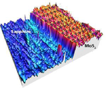
Leading provider of process solutions for a broad range of applications, Oxford Instruments is delighted to announce the development and launch of the MoS2 growth process using its high performance Nanofab nanoscale growth system.

Single layer MoS2 is a direct band gap semiconductor which has wide ranging applications in optoelectronics such as LEDs, photovoltaics, photodetectors, and bio sensors while multi layer MoS2 is an indirect band gap semiconductor which shows promise in future digital electronics.
Oxford Instruments’ scientists have undertaken extensive research and optimization of this CVD process, developed on a Nanofab system equipped with precursor delivery modules capable of delivering a wide range of liquid/solid/metal organic precursors suitable for 2D materials growth. Offering growth on a range of substrates including sapphire and ALD alumina (Al2O3 and SiO2), the system is capable of depositing other 2D transition metal dichalcogenides (TMDCs) such as WS2, MoSe2 etc.
This process development and its proven results are extremely exciting, as we enter a new phase in our 2D materials processing capabilities with the Nanofab plasma processing system. Raman analysis has demonstrated a high quality mono-layer, with AFM showing resultant smooth and uniform films. We anticipate that this development in 2D materials growth will facilitate the next generation of nano electronic devices.
Frazer Anderson, Strategic Marketing and Business Development Director at Oxford Instruments Plasma Technology
For more information please visit our webpage: www.oxinst.com/mos2
Oxford Instruments Plasma Technology offers flexible, configurable process tools and leading-edge processes for the precise, controllable and repeatable engineering of micro- and nano-structures. Our systems provide process solutions for nanometre layer epitaxial growth of compound semiconductor material, etching of nanometre sized features and the controlled growth of nanostructures.
These solutions are based on core technologies in plasma-enhanced deposition and etch, ion-beam deposition and etch, atomic layer deposition and deep silicon etch. Products range from compact stand-alone systems for R&D, through batch tools and up to clustered cassette- to-cassette platforms for high-throughput production processing.