Mar 3 2017
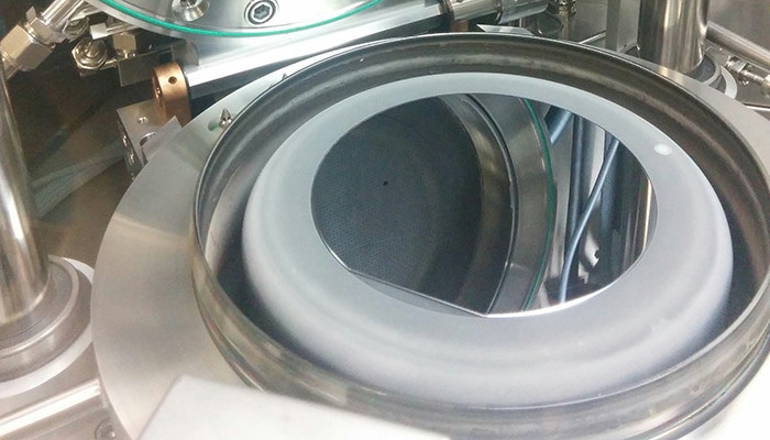
 The researchers used Micronova's cleanrooms and, in particular, a reactor designed for gallium nitride manufacturing. The image shows a six-inch substrate in the MOVPE reactor before manufacturing. Photo: Aalto University / Jori Lemettinen
Researchers at Aalto University collaborated with Okmetic Oy and the Polish ITME to study the application of Silicon On Insulator (SOI) wafers, which are used as a platform for producing a variety of microelectronics components, as a substrate for manufacturing gallium nitride crystals.
The features of gallium nitride (GaN) layers grown on SOI wafers were compared by the team with those grown on silicon substrates more typically used for the process. In addition to high-performance silicon wafers, Okmetic also produces SOI wafers, in which a layer of silicon dioxide insulator is placed between two silicon layers. The purpose of the SOI technology is to enhance the capacitive and insulating features of the wafer.
“We used a standardised manufacturing process for comparing the wafer characteristics. GaN growth on SOI wafers produced a higher crystalline quality layer than on silicon wafers. In addition, the insulating layer in the SOI wafer improves breakdown characteristics, enabling the use of clearly higher voltages in power electronics. Similarly, in high frequency applications, the losses and crosstalk can be reduced.
Jori Lemettinen, Doctoral Candidate, Aalto University
“GaN based components are becoming more common in power electronics and radio applications. The performance of GaN based devices can be improved by using a SOI wafer as the substrate”, adds Academy Research Fellow Sami Suihkonen.
SOI Wafers Reduce the Challenges of Crystal Growth
It is challenging to grow GaN on a silicon substrate. Using metalorganic vapor phase epitaxy (MOVPE), GaN layers and devices can be grown on substrate material.
Compared to a silicon wafer, while using silicon as a substrate, the grown compound semiconductor materials have varied coefficients of thermal expansion and lattice constants. These dissimilarities in their characteristics restrict the crystalline quality that can be attained and the maximum possible thickness of the formed layer.
The research showed that the layered structure of an SOI wafer can act as a compliant substrate during gallium nitride layer growth and thus reduce defects and strain in the grown layers.
Jori Lemettinen, Doctoral Candidate, Aalto University
GaN based components are typically used in white and blue LEDs. In power electronics applications, GaN transistors and diodes, especially, have gained interest, for instance in electric cars or frequency converters. It is anticipated that in futuristic radio applications, 5G network base stations will employ GaN based power amplifiers. In electronics applications, a GaN transistor provides low resistance and facilitates high power densities and frequencies.
The research paper has been accepted for publication in the journal Semiconductor Science and Technology.