Mar 12 2018
A research team headed by UCLA scientists and engineers has come up with a technique to make new kinds of artificial “superlattices” — materials made up of alternating layers of ultra-thin “two-dimensional” sheets, which are just one or a few atoms thick.
Unlike existing modern superlattices, wherein alternating layers have comparable atomic structures, and consequently similar electronic properties, these alternating layers can have drastically different structures, functions, and properties, something not formerly available.
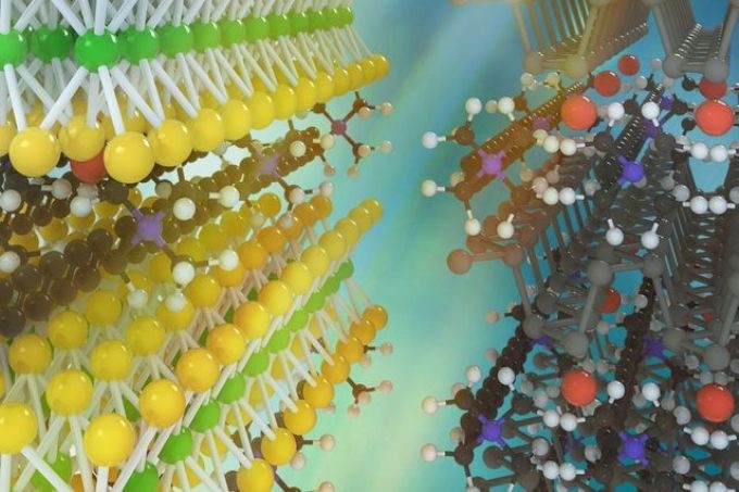
 An artist's concept of two kinds of monolayer atomic crystal molecular superlattices. On the left, molybdenum disulfide with layers of ammonium molecules; on the right, black phosphorus with layers of ammonium molecules. (Image credit: UCLA)
For instance, while one layer of this new kind of superlattice can allow a quick flow of electrons through it, the other type of layer can serve as an insulator. This design limits the optical and electronic properties to single active layers, and they do not hinder other insulating layers.
Such superlattices can form the foundation for better and new classes of optoelectronic and electronic devices. Applications include ultra-efficient and superfast semiconductors for transistors in smart devices and computers, and advanced LEDs and lasers.
In contrast to the conventional layer-by-layer assembly or growth approach presently used to build 2D superlattices, the new UCLA-led method to create superlattices from 2D materials is a lot faster and more efficient. Most significantly, the new technique easily produces superlattices with tens, hundreds, or even thousands of alternating layers, which is still not achievable with other approaches.
This new range of superlattices alternates 2D atomic crystal sheets that are interspaced with molecules of different sizes and shapes. In effect, this molecular layer becomes the second “sheet” since it is held in place by “van der Waals” forces, feeble electrostatic forces to keep otherwise neutral molecules “attached” to each other. These new superlattices are termed as “monolayer atomic crystal molecular superlattices.”
The research paper, published in Nature, was led by Xiangfeng Duan, UCLA professor of chemistry and biochemistry, and Yu Huang, UCLA professor of materials science and engineering at the UCLA Samueli School of Engineering.
Traditional semiconductor superlattices can usually only be made from materials with highly similar lattice symmetry, normally with rather similar electronic structures. For the first time, we have created stable superlattice structures with radically different layers, yet nearly perfect atomic-molecular arrangements within each layer. This new class of superlattice structures has tailorable electronic properties for potential technological applications and further scientific studies.
Yu Huang, UCLA Professor of Materials Science & Engineering
One present technique to construct a superlattice is to manually arrange the ultrathin layers one on top of the other. But this requires a lot of effort. Furthermore, since the flake-like sheets are delicate, it takes a long time to make as quite a few sheets will break during the placement process. The other method is to grow one new layer on top of the other, using a method known as “chemical vapor deposition.” But since that means a variety of conditions, such as pressure, heat, or chemical environments are necessary to grow each layer, the process could cause altering or breaking of the layer below. This technique also requires a lot of effort with low yield rates.
The new technique to develop monolayer atomic crystal molecular superlattices uses a process known as “electrochemical intercalation,” in which a negative voltage is applied. This causes negatively charged electrons to be injected into the 2D material. This, in turn, attracts positively charged ammonium molecules into the spaces between the atomic layers. Those ammonium molecules automatically accumulate into new layers in the ordered crystal structure, forming a superlattice.
“Think of a two-dimensional material as a stack of playing cards,” Duan said. “Then imagine that we can cause a large pile of nearby plastic beads to insert themselves, in perfect order, sandwiching between each card. That’s the analogous idea, but with a crystal of 2D material and ammonium molecules.”
The team first proved the new method using black phosphorus as a base 2D atomic crystal material. Using the negative voltage, positively charged ammonium ions were attracted into the base material and inserted themselves between the layered atomic phosphorous sheets.
Following that achievement, various types of ammonium molecules with varying sizes and symmetries were inserted into a series of 2D materials by the researchers. They found that they could customize the structures of the ensuing monolayer atomic crystal molecular superlattices, which had a varied range of useful optical and electronic properties.
“The resulting materials could be useful for making faster transistors that consume less power, or for creating efficient light-emitting devices,” Duan said.
The study’s lead author is Chen Wang, a doctoral student advised by Huang and Duan, who are both members of the California NanoSystems Institute. Other study authors are UCLA graduate students and postdoctoral researchers in Duan or Huang’s research groups; researchers from Caltech; Hunan University, China; University of Science and Technology of China; and King Saud University, Saudi Arabia.
The study was supported by the National Science Foundation and the Office of Naval Research.