SENTECH Instruments is a leading supplier of plasma process technology equipment for etching and deposition and thin film metrology instruments based on spectroscopic ellipsometry.
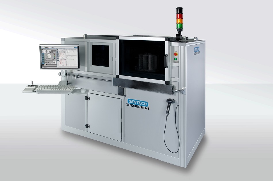
SENTECH proudly presents the SENDURO®MEMS for fully automatic metrology quality control in sensor and MEMS production. The SENDURO®MEMS provides reliable and precise measurement of thin film stacks, using spectroscopic reflectometry and ellipsometry.
Customized Measurement Equipment
The SENDURO®MEMS equipped with reflectometer is for fast thin film measurement. Combined with a spectroscopic ellipsometer measurements of film thickness and optical constants, and the analysis of multi-layer stacks are featured. The SENDURO®MEMS can be configured with μ-spot measurements in reflectometry and ellipsometry, and pattern recognition which provides the accurate measurement location. All measurements can be combined with the edge grip technology.
Highest flexibility and accuracy in terms of thin film analysis is provided by combination of spectroscopic reflectometry and spectroscopic ellipsometry based on SENTECH most accurate Step Scan Analyzer measurement mode. It is operated by the SENTECH comprehensive SpectraRay/4 software. The SECS/GEM software interface option supports the communication between factory host (MES) and production equipment (SENDURO®MEMS).
Automated Wafer Handling
The SENDURO®MEMS allows the handling of double-sided wafers. Edge grip wafer handling with small edge exclusion is optionally available for 100 mm, 150 mm, and 200 mm wafers.
The tool is equipped with robot and pre-aligner for automated wafer loading using cassettes. Single point and multiple point measurements are supported by up to 200 mm x-y mapping. Pattern recognition is available for microspot spectroscopic ellipsometry (100 x 100 μm2) and microspot reflectometry (80 μm2).
Measurement of Large Variety of Materials
The SENDURO®MEMS is a fully automated thin film metrology tool for measurement of a large variety of materials such as silicon oxide, silicon nitride, silicon oxynitride; amorphous silicon, polysilicon; photoresist, polyimide; thin metal films of Al, Pt, Cr and conductive films of TiN, TaN, TCO and ITO; single films and layer stacks of these materials on silicon wafers, silicon-on insulator substrates, silicon membranes, GaN on silicon, SiC, and more, used in MEMS and sensor production.
The SENDURO®MEMS is perfectly suited to optimize measurement speed, accuracy, and spot size by combination of ellipsometry and reflectometry in one tool. For MEMS and sensor fabrication industry this system is a cost effective asset.