May 27 2021
With attractive shapes and vivid colors, a majority of crystals are undoubtedly the wonders of nature. A few crystals are also wonders of science, with revolutionary applications in optics and electronics. Therefore, identifying an optimal way to grow these crystals is crucial to more advancements.
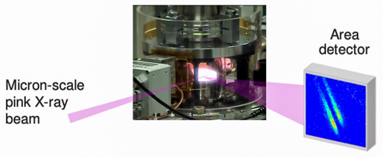
 Schematic of microbeam surface X-ray scattering during growth of gallium nitride crystal at high temperature. Image Credit: Argonne National Laboratory.
Researchers from the Argonne National Laboratory of the U.S. Department of Energy (DOE), together with three universities, have shed new light on the mechanism behind the growth of gallium nitride crystals at the atomic scale.
Today, gallium nitride crystals are extensively used in light-emitting diodes, more commonly referred to as LEDs. They could also be used to create transistors for high-power switching electronics to make smarter and more energy-efficient electric grids. The application of these “smart grids,” which could optimally balance the high power inside the overall system, may prevent power loss during extreme storms.
Furthermore, the same kind of technology could render individual homes more energy efficient. It could even be used in optical communications in which lasers send data. This data transfer can be faster, more accurate, and more secure than present-day capabilities.
Due to these various applications, researchers around the world have been working to enhance the method for growing gallium nitride crystals.
Gallium nitride has a more complicated crystal structure than silicon, the typical crystalline material in electronics. When you grow this crystal, you thus get more fascinating behavior at the surface.
G. Brian Stephenson, Distinguished Fellow, Materials Science division, Argonne National Laboratory
At the atomic scale, the surface of a growing gallium nitride crystal generally resembles a staircase of steps in which each stair represents a layer of a crystal structure. To the growing crystal surface, atoms are added by attaching them to the boundaries of the steps. Due to the structure of the gallium nitride crystal, the steps have alternating edge structures, which are marked as A and B.
The varied atomic structures resulted in varied growth behaviors of the A-type and B-type steps. A majority of the theoretical models denote that atoms build up faster on a B-type step; however, experimental confirmation is not available.
Because of the high temperatures and chemical atmosphere involved, it is not possible to examine the growth of gallium nitride with a standard electron microscope and test the model prediction.
G. Brian Stephenson, Distinguished Fellow, Materials Science Division, Argonne National Laboratory
For this reason, the researchers sought the help of the Advanced Photon Source (APS), a DOE Office of Science User Facility at the Argonne National Laboratory. At the APS, the intense energy of the X-rays with a beam measuring just a few micrometers wide (beamline 12-ID-D) enabled the researchers to track the speed of the growth of gallium nitride on the crystal surface steps.
Such X-rays serve as the perfect probe because they are not only sensitive to the atomic-scale structure but can also enter the crystal environment at increased temperatures, that is, more than 1400 °F, while it is growing.
“Based on modeling, many had assumed that atoms probably build up faster on the type-B step. Imagine our surprise when it turned out to be step A. This suggests the chemistry of the growth process may be more complicated than previously thought,” added Stephenson.
This work is a great example of the importance and power of probing a material while a process is underway. Quite often when we use such probes to study processes like synthesis, we find the story to be more complex than we originally thought and counter to conventional wisdom.
Matt Highland, Physicist, X-ray Sciences Division, Argonne National Laboratory
The outcomes have evident implications for improving the present interpretation of the atomic-scale mechanisms of the growth of gallium nitride. This interpretation also has major practical implications for designing sophisticated gallium nitride devices by enabling better control of the incorporation and growth of more elements for enhanced performance.
The results can also be used for growing similar crystals, such as host semiconductor materials meant for quantum information science.
The study was funded by the DOE Office of Basic Energy Sciences and has been published in the Nature Communications journal.
Apart from Stephenson and Highland, other authors from the Argonne National Laboratory include Guangxu Ju, Dongwei Xu (currently at Huazhong University of Science and Technology), Eastman, and Peter Zapol. University participants include Carol Thompson from Northern Illinois University and Weronika Walkosz from Lake Forest College.
Journal Reference:
Ju, G., et al. (2021) In situ microbeam surface X-ray scattering reveals alternating step kinetics during crystal growth. Nature Communications. doi.org/10.1038/s41467-021-21927-5.