About 54.6 million tons of electronic waste worth USD 57 billion was generated in 2019 worldwide. Only 17.4% of global electronic waste is formally collected and recycled and the majority of the waste remains not formally tracked or recycled.
PCBs, being a huge share of electronic waste, can be considered as a secondary value recovery resource due to the presence of high concentrations of precious and base metals. PCBs are highly heterogeneous and their composition can vary significantly based on their original function. Currently, no standard methods exist for PCB characterization that can help gather information relevant to value recovery operations.
This work compares multiple analytical methods for the characterization of the metal content in PCB samples. It also evaluated smelting and ashing as possible pre-treatment methods before acid digestion. The researchers used a mixed-metal standard (MMS) to determine the accuracy of the methods.

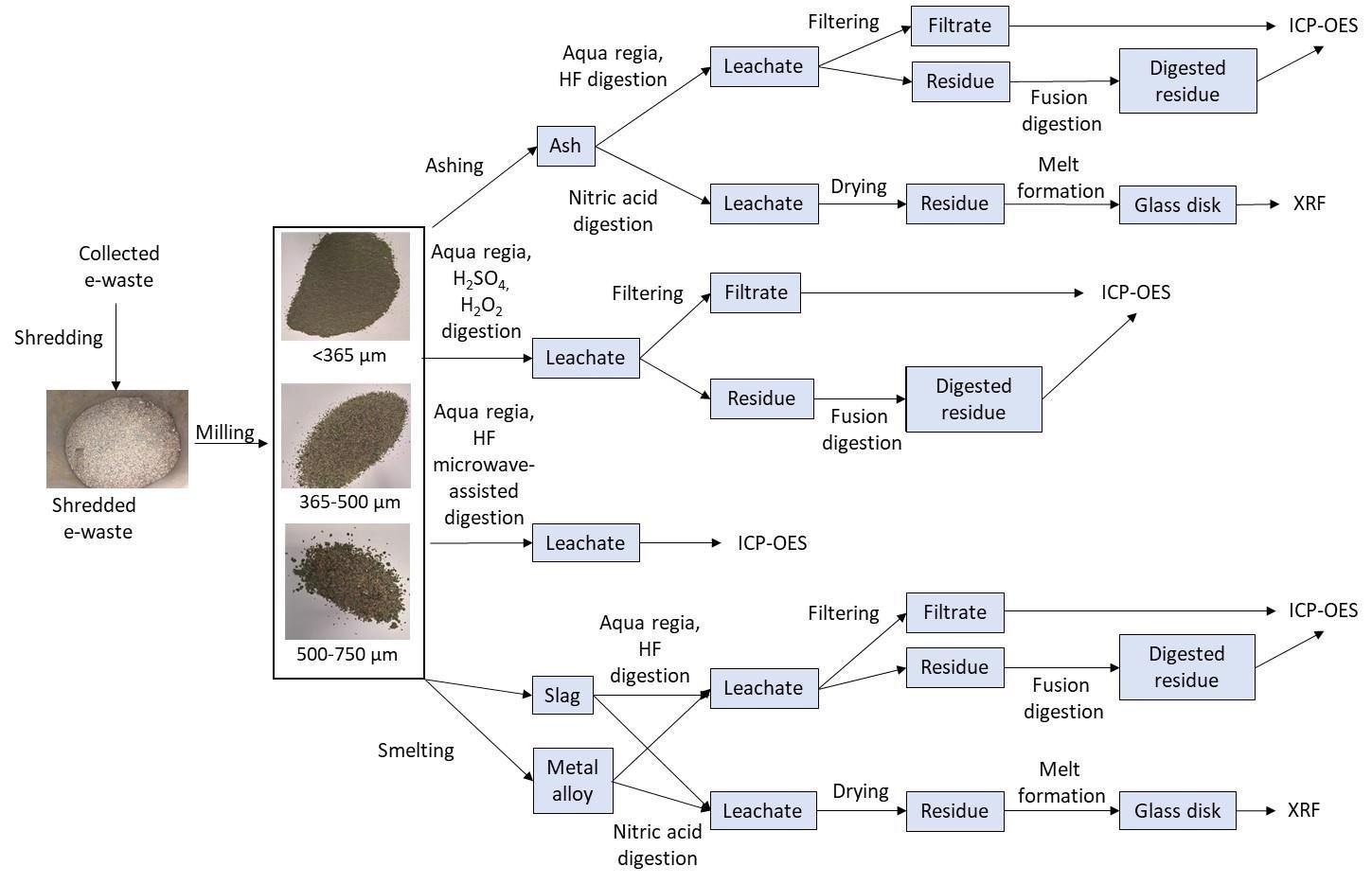
Flowsheet for sample processing and analytical methods examined. Image Credit: Van Yken, J/Shutterstock.com
About the Study
In the study, four different analytical methods were used to process samples to assess the effect of particle size and element-specific effects on PCB characterization. The PCBs were ground and sieved to three size fractions: <365 μm, 365–500 μm, and 500–750 μm, which were then individually subsampled to obtain representative elemental analysis samples. Mixed-metal standards were then weighed, mixed with composite samples, and then analyzed.
Three replicate samples from each size fraction were subjected to all the analytical methods used in the study to determine their element contents. The total elemental content for the whole PCB batch was calculated. Ashed PCB waste was slightly “sintered” and broken up prior to sub-sampling for chemical analysis and the loss on ignition (LOI) was calculated.
After smelting the PCB samples, the elemental composition of each phase was analyzed separately, which in turn was used to measure the original PCB samples’ metal content.
Analytical characterization methods used in the study include the following: 1. multi-acid digestion followed by inductively coupled plasma optical emission spectrometry (ICP-OES) analysis, 2. nitric acid digestion followed by analysis by X-ray fluorescence (XRF), 3. multi-acid digestion followed by fusion digestion and ICP-OES analysis, and 4. microwave-assisted multi-acid digestion followed by analysis using ICP-OES.

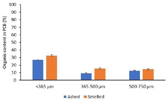
The organic content of PCB samples as calculated based on loss on ignition (LOI) during smelting and ashing pre-treatments. Error bars show standard deviations between three replicate samples. Image Credit: Van Yken, J/Shutterstock.com
Results of the Study
Overall, Cu was the most abundant metal in the PCBs, with content ranging between 12.18 and 58.93% depending on the method used and the particle size. The contents of Al, Fe, Sn, Ni, and Zn across various particle sizes were in the following ranges, respectively: 1.97–14.1%, 0.13–3.17%, 0.05–1.57%, 0.22–0.97%, and 0.005–0.94% depending on the analytical methods used.
Smelting was shown to reduce the accuracy of further analysis because some metal species were volatile at high temperatures, while ashing was found to be an effective pre-treatment method. While smelting allowed for larger sample sizes, ashing offered an alternative for the combustion of the organic material without the volatilization of metal species.
Microwave-assisted multi-acid digestion was found to be the most precise and accurate method out of the four analytical methods tested in this study and had the lowest relative standard deviation (RSD). This method can be further improved by increasing the number of replicates and the sample mass.

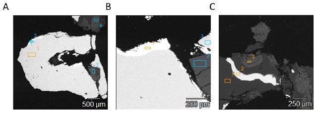
Scanning electron microscopy (SEM) images showing specific locations of the resin block (A–C) used for determining the elemental composition of PCBs for <365 µm fraction size with energy-dispersive X-ray spectroscopy (EDS) analysis as shown in Table 4. Details on the specific spectral peaks at these locations can be found in Supplementary Figures S1–S3. Image Credit: Van Yken, J/Shutterstock.com
Conclusions
The characterization of PCB waste is critical to understanding the composition of the boards, which will help evaluate the efficiency of metal extraction processes. The metal, plastic, and ceramic content of PCBs can significantly vary depending on the particle sizes with smaller particles sizes leading to lower RSDs during metal content analysis compared to larger particle sizes.
According to the study results, microwave-assisted multi-acid digestion showed the highest degree of accuracy out of all methods tested. Further research is needed to produce a reference material that matches the complexity of the waste PCB material.
This work highlighted the significance of understanding PCB composition and the selection of appropriate analytical methods. Proper selection of analytical methods can: help gain a better understanding of the input material, greatly affect the accuracy of the PCB metal content, and also enable accurate tracking of various metal species during the metal extraction process.
Disclaimer: The views expressed here are those of the author expressed in their private capacity and do not necessarily represent the views of AZoM.com Limited T/A AZoNetwork the owner and operator of this website. This disclaimer forms part of the Terms and conditions of use of this website.
Source:
Van Yken, J.; Cheng, K.Y.; Boxall, N.J.; Sheedy, C.; Nikoloski, A.N.; Moheimani, N.R.; Kaksonen, A.H. A Comparison of Methods for the Characterisation of Waste-Printed Circuit Boards. Metals. 2021, 11, 1935. https://www.mdpi.com/2075-4701/11/12/1935