 By Surbhi JainReviewed by Susha Cheriyedath, M.Sc.Oct 12 2022
In an article recently published in the open-access journal Scientific Reports, researchers discussed the utility of electrostatically sprayed carbon electrodes for high-performance organic complementary circuits.

Study: Electrostatically-sprayed carbon electrodes for high performance organic complementary circuits. Image Credit: OliveTree/Shutterstock.com
Background
One of the most crucial components in electronic circuits is thin-film transistors (TFTs), whose performance is heavily influenced by heterointerfaces between different materials. Sequential deposition of these components is required by TFT manufacturing procedures, which is expected to hinder the reliable fabrication of integrated devices.
Heterointerface engineering can be especially harmful to TFTs made of solution-processable organic semiconductors (OSCs). The performance of solution-processed organic thin-film transistors (OTFTs) has been advancing due to recent advances in chemistry and printed electronics device engineering. Excellent environmental stability and reasonably high field-effect mobilities have been attained for single-crystalline thin films made of a few monolayers of OSCs.

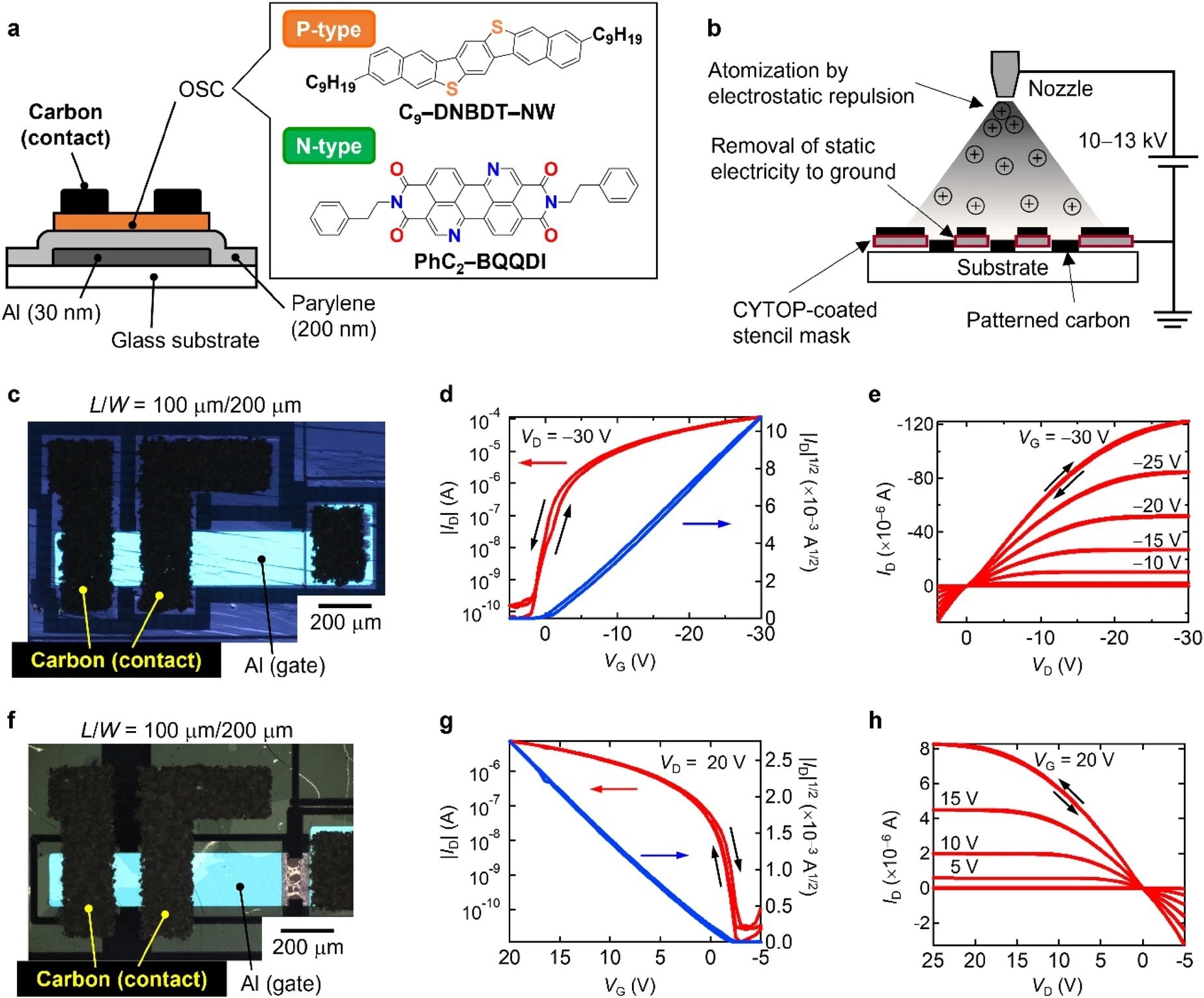
Configuration and transistor characteristics of p- and n-type OTFTs with carbon contact electrodes. (a) Device configuration of OTFTs with carbon contact electrodes, in which a single-crystalline thin film of either p-type C9–DNBDT–NW or n-type PhC2–BQQDI was employed as the OSC layer. (b) Schematics of electrostatic spray coating of a carbon suspension including graphite powder and carbon black. The carbon suspension was atomized by electrostatic repulsion due to the charging nozzle to which a high voltage of 10–13 kV was applied. The carbon was patterned on a target substrate through a CYTOP-coated stencil mask. (c) Transfer characteristics in the saturation regime (VD = − 30 V) and (d) output characteristics of a p-type OTFT including C9–DNBDT–NW as the OSC layer and carbon as the contact electrodes. (e) Polarized optical microscopy (POM) image of the p-type OTFT under cross-Nicol condition. (f) Transfer characteristics in the saturation regime (VD = 20 V) and (g) output characteristics of the n-type OTFT with PhC2–BQQDI as the OSC layer and carbon as the contact electrodes. (h) POM image of the n-type OTFT under cross-Nicol condition. The channel length (L) and width (W) of both OTFTs were 100 μm and 200 μm, respectively. Image Credit: Watanabe., Scientific Reports
Large crystalline membranes can now be produced thanks to improved manufacturing techniques. OTFTs often call for the sequential deposition of metal electrodes on top of or around the edges of the OSC thin films. It is known that the carrier injection characteristics and interfacial contact resistance are particularly influenced by the aspects of the gold/OSC interface. There have been few studies on alternatives to gold electrodes, which is a barrier to low environmental loading and cost reduction in printed, flexible electronics.
About the Study
In this study, the authors showed that electrostatic spray coating could be used to directly install and shape graphite-based carbon electrodes onto an organic single-crystalline thin film. With no appreciable degradation during electrostatic spray operations, the current OTFTs displayed reasonably high field-effect mobility values of up to 11 cm2 V-1 s-1 for p-type and 1.4 cm2 V-1 s-1 for n-type. The study discussed a complementary circuit, an inverter made of n- and p-type OTFTs, and an operational metal-free OTFT made entirely of carbon-based materials.
The team elucidated that single-crystalline OSC thin films could be directly coated with graphite-based carbon, patterned, and used as an effective contact electrode for both p- and n-type OTFTs. With high field-effect mobilities, negligible hysteresis, a close to zero turn-on voltage, and an on-off current ratio of roughly 106, the OTFTs exhibited excellent transistor characteristics that were comparable to the gold-contact OTFTs. In addition, one of the first organic complementary circuits to work with carbon electrodes based on graphite was a complementary inverter made up of n- and p-type OTFTs that was successfully operated at a supply voltage (Vdd) of 5–15 V.

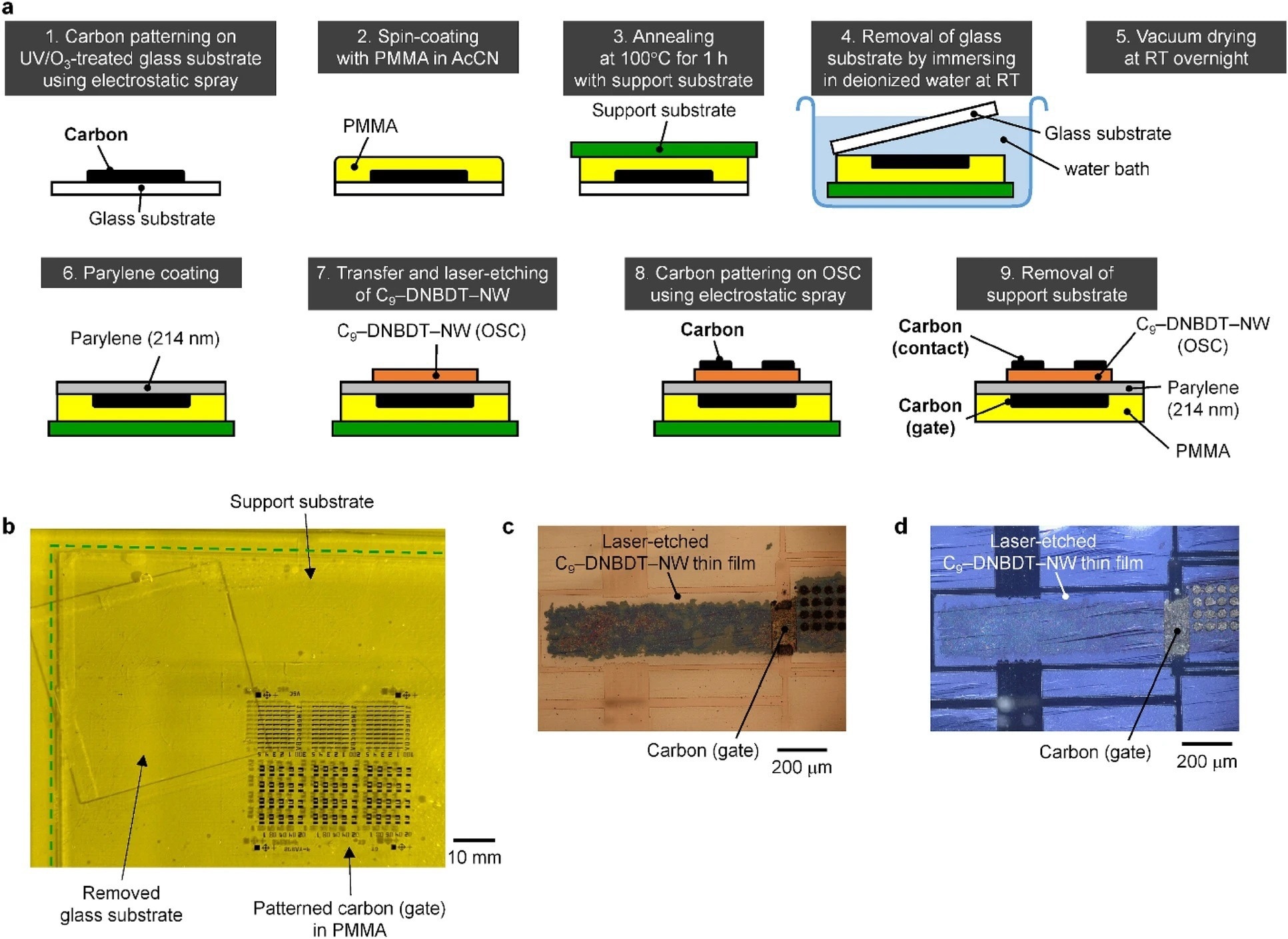
Fabrication of metal-free OTFTs. (a) Sequential fabrication procedure of a metal-free OTFT composed of C9–DNBDT–NW as the OSC, carbon as the contact and gate electrodes, parylene as the hydrocarbon polymeric insulator, and PMMA as the substrate. (b) Photo of a patterned carbon/PMMA film being removed from a glass substrate in a water bath. (c, d) POM images of a C9–DNBDT–NW thin film transferred onto a parylene/carbon/PMMA film and then laser-etched. Observed under (c) open-Nicol and (d) cross-Nicol conditions, respectively. Image Credit: Watanabe., Scientific Reports
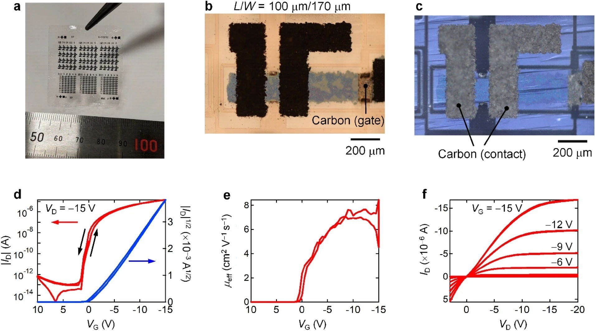
The researchers used an OTFT without any metals that were made entirely of carbon-based components, including OSCs, organic polymer insulators, carbon contact/gate electrodes, and organic polymer substrates.
Observations
With high effective field-effect mobilities of 11 cm2 V-1 s-1 for the p-type OTFTs and 1.4 cm2 V-1 s-1 for the n-type OTFTs, respectively, the resulting n- and p-type OTFTs demonstrated excellent transistor properties. These traits were comparable to those of typical OTFTs with gold contact electrodes, which showed that carbon could be used in place of less expensive, more readily available metals like silver, gold, and platinum to make efficient contact electrodes for OTFTs.
The current carbon suspension could be applied to offset and inkjet printing, among other printing processes. Graphite powder had an average particle size of 3 μm. More delicate patterning was made possible by further particle size reduction, which would be a major problem in the future. An inverter made of n- and p-type OTFTs with supply voltages ranging from 5 to 15 V was operated satisfactorily.
Extending the nozzle scanning distance made it simple to increase the spray-coated area, and the carbon electrode was successfully patterned on a substrate with dimensions of 50 mm by 50 mm.

Characteristics of metal-free OTFTs. (a) Photo of metal-free OTFTs on a 30-mm by 30-mm self-standing PMMA film. (b, c) POM images of the metal-free OTFT under (b) open-Nicol and (c) cross-Nicol conditions, respectively. (d) Transfer curve in the saturation regime (VD = − 15 V), (e) corresponding effective mobilities plotted as functions of VG, and (f) output curve of the metal-free OTFT. Image Credit: Watanabe., Scientific Reports
Conclusions
In conclusion, this study created a technique using electrostatic spray coating to pattern graphite-based carbon contact electrodes onto p- and n-type single-crystalline OSC thin films without suffering significant damage. The team also created and used a carbon-based OTFT made up of a poly(methyl methacrylate) (PMMA) substrate, carbon electrodes, a p-type OSC, and hydrocarbon polymeric insulators. They stated that carbon electrodes could be used to fabricate metal-free integrated circuits, and OTFT applications in flexible, printable electronic devices would therefore advance further.
The authors also mentioned that the findings of this study mark a significant advancement in the creation of printed metal-free integrated circuits and serve as a foundation for continued research and development of complementary printed integrated circuits.
References
Watanabe, K., Miura, N., Taguchi, H., et al. Electrostatically-sprayed carbon electrodes for high performance organic complementary circuits. Scientific Reports, 12, 16009 (2022). https://www.nature.com/articles/s41598-022-19387-y
Disclaimer: The views expressed here are those of the author expressed in their private capacity and do not necessarily represent the views of AZoM.com Limited T/A AZoNetwork the owner and operator of this website. This disclaimer forms part of the Terms and conditions of use of this website.