3D optical profiling integrates imaging with accurate speed and measurement, which is not possible with contact techniques like atomic force microscopes (AFMs) or stylus profilers.
3D optical profilers are used for a range of measurements such as sub-micron to nanometer level surface roughness and multi-millimeter step heights.
Optical profilers are normally designed on sophisticated optical microscopes offering the dual benefit of excellent imaging and no contact with the measured surface. They use several light sources normally with high-brightness LEDs in order to light the sample and advanced cameras to capture images that are converted to height information using interferometry or confocal microscopy techniques.
Optical profilers are currently deployed in a number of high-technology industries where the surface properties of materials are studied. Characterization of advanced semiconductor packaging, solar panels, high-brightness LEDs, and microfluidic devices are some of the applications where this technique is being used.

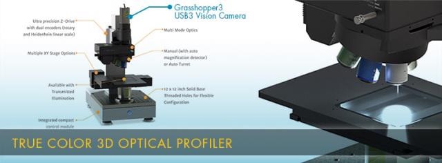
Figure 1. The Zeta-20 uses the Grasshopper3 and produces true color 3D optical images with multi mode optics technology

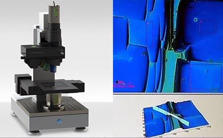
Figure 2. Zeta-20 and image sample
Improvements in Image Capture Enable New Techniques and Lower Costs
The Zeta-20 was introduced recently. The Zeta-20 is designed based on a patented optical technique known as ZDot™ that allows it to capture and study images of tough to measure surfaces in a manner not feasible with conventional techniques such as laser confocal microscopy or interferometry.
These surfaces include multi-layer and transparent surfaces, those with low-contrast and low-reflectivity or those having high roughness.
The Zeta-20 optical profiler features a solid optical base plate having threaded holes offering flexibility to the user to position any sample to be studied under several objective lenses. Using lenses with a range of magnifications, users can see the impact on the field of view of the sample obtained using the instrument. The depth of focus can also be visualized, which changes with the numerical aperture of the actual objective used.
The 3D image of a sample is created by illuminating using a high-intensity white light LED source to ensure that the color of the sample is retained. The relative distance between the sample and the objective lens selected by the user is altered, controlled by a PC through several pre-determined steps with a precision closed loop z-drive having linear and rotary encoders.
Zeta Tencor 20 Using Bright LEDs
At each stage, a dot pattern is formed by a custom-designed electronic pattern generator and is projected on the focal plane of the objective lens and using a Point Grey Grasshopper3 GS3-U3-28S5C 2.8M pixel color camera, an image is captured of the sample.
The pattern is then removed from the focal plane of the instrument and a second image of the sample is captured by the camera. Both image sets captured are transmitted to a PC over a USB3 Vision interface where the images are analyzed using a proprietary software algorithm to form a 2D composite image and a true color 3D image of the sample. Since the system determines when the dot pattern is in focus on the sample, it is understood that the sample also will be in focus. The method allows precise and consistent 3D imaging on almost all samples irrespective of its image contrast.

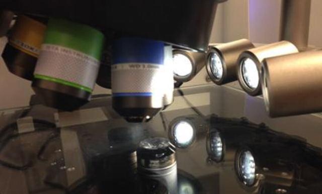
Figure 3. High intensity white light LEDs preserve the color of the sample
Zeta 3D Uses the Grasshopper3 Camera
VP, Special Projects at KLA, Ken Lee stated that the Point Grey camera is an essential building block in the Zeta-20 3D optical profiling system. The camera works in tandem with the company’s patented ZDot pattern generator, enabling sample images to be captured by the instrument at 1920 x 1440 pixel resolution, enabling customers to observe sample features at a spatial resolution of below 0.5µm.

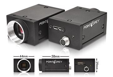
Figure 4. Grasshopper3, Sony ICX674 CCD, 2/3", 4.54 µm, 1920 x 1440 at 26 FPS
Software Analysis
On capturing the sample’s 3D image by the optical profiler, a Windows-based software package provides the user with 3D images of the sample, a two-dimensional composite image and a window wherein the results of studying the sample using the tool in the software package can be observed on-screen. The analysis tools enable step height measurements on the sample surface to be performed and also help identify the difference in the average height between two positions on the sample surface.
The software can also determine the surface roughness of the sample material. Surface roughness is a key parameter for studying material surfaces as it impacts their properties.
Since the Zeta 3D optical profiler can take a number of measurements on almost any surface, it is not sensitive to vibration and allows measurements that are not possible with confocal microscopes or interferometers. It also has been extensively adopted at a number of leading universities and research and development labs, and universities like the Fraunhofer Institute, the NIST, Yale, MIT and Purdue and also in LED, solar and global semiconductor companies.

Figure 5. The Zeta-20 is capable of measuring multiple dimensions, including 2D and 3D roughness, micro-CMM, film thickness, step heights, wall angles and more

This information has been sourced, reviewed and adapted from materials provided by KLA.
For more information on this source, please visit KLA.