Optical profilers are utilized in a wide range of industries to carry out accurate 3D measurements. However, the majority of these technologies come with certain limitations. This article compares the unique benefits of the patented ZDot™ optical profiling technology by KLA with other standard confocal laser scanning microscopy (CLSM). Table 1 shows a comparison of imaging, cost, samples and operation modes between the ZDot™ technology and a traditional CLSM.
Table 1. ZDot™ and traditional CLSM
| |
ZDot™ |
Confocal |
| Imaging |
Confocal Grid Structured Illumination |
Scanning Confocal |
| Cost |
Low initial cost
Noperiodic maintenance required |
High initial cost
Periodic maintenance required |
| Samples |
Wide variety
(widest among all optical profilers) |
Moderatevariety |
| Operationmodes |
ZDot™, Interferencecontrast, Interferometer, Film Spectrometer, Diamond Scribe, Dark Field, Through TransmissiveIllumination |
Confocalbright field
Interference contrast |
Evolution of Optical Profiling Technology
- The concept of confocal microscopy was first developed in 1957 by Marvin Minsky. This technique allowed optical sectioning in the “Z” dimension by utilizing a pinhole to perceive the light from one focal plane. However, this method presented a number of challenges such as high sensitivity to vibration, extended exposure times and the need for a slow, regular raster.
- Laser scanning process was developed in 1978 by Thomas and Christophe Cremer. Technological advancements included digital image reconstruction, 3D laser scanning, as well as fast and more precise imaging. However, this method also included certain drawbacks such as high sensitivity to vibration, no true color data, requires image artifacts from a coherent nature of laser and also requires periodic adjustments and trained users.
- Confocal grid structured illumination (CGSI) was developed in 2009 by James Xu and Ken Lee. This technique eliminates periodic alignment, provides true color information without coherent artifacts in the image and offers a lower cost of ownership.
- 3D optical profilers developed by KLA are one step ahead of these technologies. They can determine surface roughness from Å to mm and measure step height, spanning from nm to mm. Although the Zdot™ technology is similar to confocal microscopy, it utilizes white light. This allows concurrent true-color imaging and sensitive height measurement.
Advantages of ZDot™ Technology
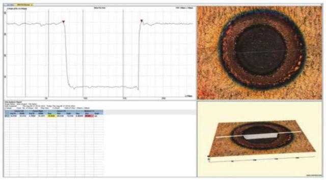
Confocal laser scanning microscopy uses a laser light source to image surfaces. Since the detector has a single wavelength input, its rebuilds a black and white image based on the intensity of the signal returned and this image is falsely colored to expose the height information (Figure 1). Artifacts in the reconstruction arise from the coherent nature of the laser, restricting its application to specific sample types. All these issues are resolved by ZDot™ technology, which removes the necessity for scanning and uses high-brightness LEDs (HBLEDs) as a light source. In defect analysis, true color imaging proves particularly useful.

Figure 1. Blind via hole critical dimensions
Since the Zeta-300 optical profiler is insensitive to vibration, it allows for precise and repeatable measurements. Present-day measurement maintains the system in a continuous production-ready state. The instrument also eliminates the need for periodic adjustment, which is crucial for a scanning confocal microscope. KLA provides various paths to automation, ranging from a custom chuck or a motorized stage on a KLA Zeta-20 instrument through to a complete, automated wafer robot system on the Zeta-300 optical profiler.
Extending the concept of confocal microscopy, the ZDot™ optical profiling technology offers the advantage of true-color imaging. Furthermore, complex surfaces can be imaged without any major issues. This feature allows excellent metrology capability for challenging research and development and manufacturing applications in the HBLEDs, sophisticated microfluidics, solar cells, semiconductor packaging, and numerous other industries.
Applications for the Zeta-300 Optical Profiler
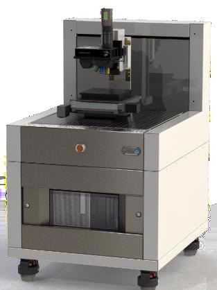
The Zeta-300 optical profiler (Figure 2) is used in the following applications:
- Solar roughness and defects: ZDot™ technology provides data regarding numerical roughness and gives both true and false color imaging for defect analysis.
- MEMS device inspection: ZDot™ examines low temperature MEMS sensing device of Argonne National Lab rapidly and in color.
- Surfaces with high slope: ZDot™ technology can image high slope image surfaces such as the side wall and chamfer of a semiconductor wafer.
- Solar devices and substrates: Zeta optical profilers exhibit true film colors and are capable of handling different materials in the same field of view.

Figure 2. The Zeta-300 is a good choice for automation
Accessories
KLA optical profilometers include the following accessories:
- External dark field illumination
- Diamond scribe to mark defects
- Edge inspection fixture with dark field illumination
- Swivel head option
- Through transmissive illumination
Conclusion
Although KLA’s ZDot™ optical profiling technology resembles a confocal microscopy, it employs a white light, providing true-color imaging and sensitive height measurement at the same time. The range of applications along with extensive accessories makes KLA optical profilometers an instrument of choice for accurate 3D measurements.

This information has been sourced, reviewed and adapted from materials provided by KLA.
For more information on this source, please visit KLA.