In order to avoid progressive contamination of samples and vacuum chamber surfaces during analysis and characterization of nanocrystalline materials and nanostructures, in-situ plasma cleaning is essential.
For effectively and rapidly eliminating hydrocarbon contamination from samples and vacuum chambers, a necessary accessory is a plasma cleaner.
The Evactron plasma radical source operates at turbopump pressures and can generate a low temperature RF plasma using its unique RF hollow cathode, allowing it to create oxygen radicals when air is the feed gas.
The pumping system removes gaseous phases formed by surface hydrocarbons combining with the oxygen radicals.
Plasma cleaning has many benefits, including no damage to EDS detectors or x-ray windows due to oxygen radial generation, prevention of hydrocarbon deposition during imaging, improved image quality of serial block-face SEM volumetric sets and faster pump-down times.
Two types of scanning electron microscope (SEM) techniques that can be used to characterize the microstructures of crystalline materials on the nano- and micro-scale are transmission Kikuchi diffraction (TKD) and electron backscatter diffraction (EBSD).
The diffraction patterns originate from very close to the sample surface, meaning that in order to obtain good TKD and EBSD results, specimen preparation is critical; a surface free from preparation-induced dislocations and contamination is necessary.
When analyzing nanostructured materials, use of the superior spatial resolution of TKD is preferred. The accumulated electron dose (here meaning the electron dose per square micrometer) is extremely high because of the relatively weak diffracted signal and the small measurement step size.
The effectiveness of the technique is reduced by the likelihood of drift and contamination.
A nanostructured Ni sample was analyzed using TKD to investigate the benefits of plasma cleaning for these kinds of experiments – the test used an analysis speed of approximately 66 patterns per second (using a CCD-based EBSD detector) and a 4 nm step size.
The data was processed using AZtecCrystal, a Nordlys Nano EBSD detector and a Zeiss Ultra Plus FEG-SEM using Oxford Instruments Aztec EBSD system. No plasma cleaning was carried out for the first analysis.
Then, for the second analysis, the sample was plasma cleaned within the microscope chamber for 5 minutes prior to the investigation, although the exact same electron beam and EBSD detector settings were used as in the first analysis.

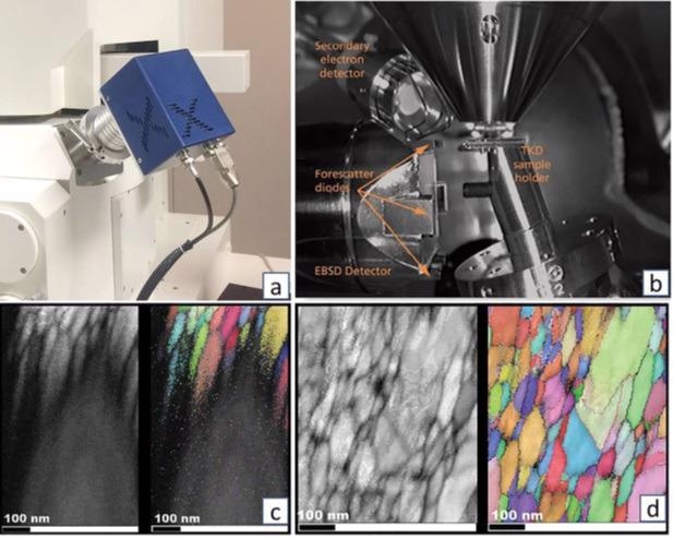
Figure 1. Image Credit: Evactron (XEI Scientific)
An Evactron E50 mounted on an SEM chamber port is shown in Figure 1a; this is the most recent addition to the XEI Scientific product line.
Figure 1b shows how an electron-transparent sample is placed at a short working distance (5-7 mm) for TKD experiments, putting it just above the top of the EBSD detector’s phosphor screen.
Figure 1c demonstrates the results from the first test, where there was no plasma cleaning prior to analysis.
It shows that although there was initially good indexing, contamination built up, and the quality of the pattern decreased rapidly, showing a correspondence with a drop in indexing.
Noticeable sample drift also occurs – this causes a perceived stretching of grain shapes. Figure 1d shows the second analysis, done following in-chamber plasma cleaning.
In this analysis, there was consistently good indexing throughout the analysis and no degradation of pattern quality. There was minimal data processing but effective characterization of the microstructure with an observed minor drift.
Plasma cleaning, combined with the latest generation of fiber-optic coupled CMOS EBSD, which are higher sensitivity, could enable significantly higher resolution analyses and/or higher speed. This is because of the lack of service degradation and relative improvement in the quality of the diffraction patterns.
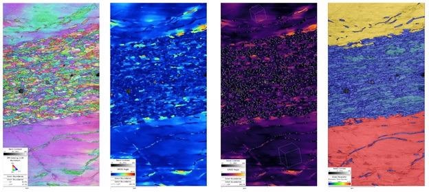
The results shown in Figure 2 can be replicated by using optimal sample preparation followed by in-situ plasma cleaning – the image shows a highly deformed AI alloy containing a nanocrystalline shear band showed in a high-resolution TKD map.

Figure 2. (a) Orientation map using the inverse pole figure (surface normal) coloring scheme. (b) Grain relative orientation deviation (GROD) map superimposed with grain boundaries. (c) Grain relative orientation deviation (GROD) map superimposed with 3D representations of the unit cell orientation of each grain. (d) Grain size map (equivalent circle diameter) with superimposed grain outlines. In all images, the scale bar marks 5 um, and the maps were collected using a measurement step size of 7.5 nm. Image Credit: Evactron (XEI Scientific)
Many advantages were demonstrated here in plasma cleaning a sample prior to TKD experiments.
Extended experiments need enhanced measurement efficiency and improvement in pattern quality, which can include multiple and fast scans of the same sample position – such as for repeated analyses for in-situ straining or heating experiments.
Plasma cleaning has many advantages and is recommended for all high-resolution EBSD and TKD experiments. The process cleans the holder, detectors, and chamber simultaneously, which is why plasma cleaning the sample inside the microscope chamber is recommended.
References and Further Reading
- Patrick Trimby (2012) Orientation mapping of nanostructured materials using transmission Kikuchi diffraction in the scanning electron microscope. Ultramicroscopy 120: 16-24
- Ewa Kosmowska et al., (2017) Improved Pump Down Time with Evactron® Turbo PlasmaTM Cleaning. Microsc. Microanal. 23 (Suppl 1): 74-75.
- Barbara Armbruster et al., (2017) Plasma Cleaning Improves the Image Quality of Serial Block-face Scanning Electron Microscopy (SBFSEM) Volumetric Data Sets. Microsc. Microanal. 23 (Suppl 1): 1266-1267.

This information has been sourced, reviewed and adapted from materials provided by XEI Scientific.
For more information on this source, please visit XEI Scientific.