How Optical Polishing Helps Improve Surface Quality
Optical polishing is a method in manufacturing that was specifically developed with the aim to minimize the number of defects and optimal micro-roughness values. The process of polishing necessitates the use of free grains typically suspended in a liquid (slurry), rather than being fastened to a wheel, as in grinding. This methodology can produce exceptionally smooth surfaces with roughness values below 1 Å, which can significantly limit scattered light below the 1 ppm level, which is a critical aspect when optics are used in transmission or as an effective substrate for improved coating adhesion
High precision optical components are fabricated from various materials, such as glass, composites, ceramics, and metal to name a few. For high-performance optical applications, the prevalent optical polishing techniques yield surfaces of desired standards.
The higher-grade surface finish capacity of polishing has led to the widespread acceptance of this for the manufacture of precision optical and mechanical components.
Each optics manufacturer will have unique considerations relative to the standard polishing method, as well as having proprietary techniques to reach distinct goals. For instance, various materials will act differently to contrasting spindle or lap speeds. So, the consistency of the slurry’s small abrasive particle sizes flowing over the optical surfaces needs to be considered.
Additionally, factors regarding how time affects the polishing process; the impact of larger particle sizes; and outside contamination causing scratches or damage to the surface are also evaluated.
It is therefore vital to pay close attention to detail across all aspects of the polishing process. All factors including handling, electrical charge, spindle or lap speeds, particle size distribution in the slurry, polish time and even monitoring the chemistry of the slurry can have a significant impact on the final quality of the surface.
This can prove to be exceptionally difficult when consistency is required to achieve super smooth surfaces
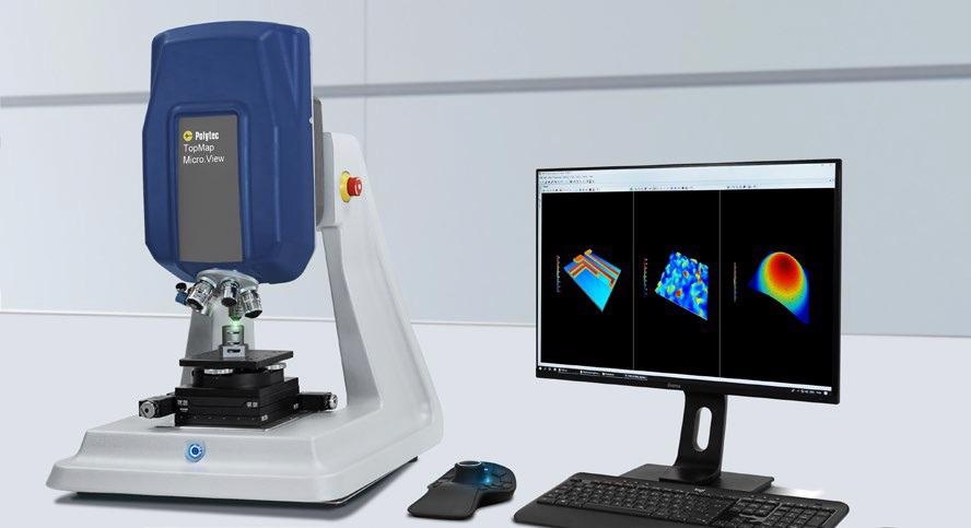
Polytecs TopMap Micro.View® coherence scanning interferometer. Image Credit: Polytec
Optical 3D Surface Profiling with a TopMap Micro.View®
The TopMap Micro.View® is Polytec GmbH’s non-contact optical metrology tool. It is a state-of-the-art measurement tool that combines advanced technology with the ability to measure and characterize surfaces to precise international standards and traceable artifacts with excellent stability.
Quality control places high demands across the optics industry, and for super finished surface texture, non-contact inspection of the 3D topography is deemed necessary.
Other than the sub-nanometer sensitive Z-resolution, this coherence scanning interferometer (CSI) also demonstrates high repeatability. Alongside automated software and a stable hardware platform, Polytec’s TopMap optical profilers provide areal surface topography characterization.
For the measurement and characterization of precision-made, optically smooth surfaces, the TopMap Micro.View® is perfectly optimized. All parameters for the TopMap Micro.View® is in compliance with ISO 4288 and ISO 25178.
The definitions used in Polytec datasheets (and the Fair Data Sheet) are provided in the latest ISO 25178-600. Instruments also follow ISO 25178-700 (calibration of areal measuring instruments) standards, and the description corresponds with Polytec’s specifications.
Surfaces can also satisfy the optical elements within ISO 10110, which includes surface texture measurements with accurately filtered parameters, measurement of surface imperfections, scratches, chips and digs can be evaluated and the relative data displayed.
Measurement Examples
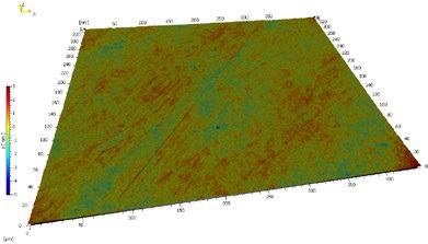
Measurement of a polished silver mirrored unfiltered data showing fine 1 nm processing marks on the surface. Sa = 0.29 nm, Sq = 0.38 nm. Image Credit: Polytec
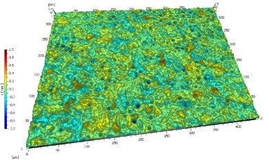
Measurement of a polished silicon surface correctly analyzed with correct filtering as recommended by ISO 10110. Sa = 0.065 nm, Sq = 0.089 nm. Image Credit: Polytec
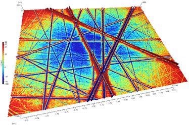
Polished glass showing 44 nm scratch damage. Sa = 2.81 nm, Sq = 4.25 nm. Image Credit: Polytec
Summary
The new TopMap Micro.View® is optimally suited for optical polishing applications. This instrument utilizes state-of-the-art coherence scanning interferometry and will also demonstrate the ability to function as a key process optimization tool across a production facility. All measurements can be fully automated and are non-contact to limit any handling errors.
Measurements Offer:
- Accurate and quantitative surface characterization
- Fast, convenient and optionally fully automated
- High resolution, highly repeatable and stable measurements
- Non-destructive – no sample contact or preparation is required
- Works for a wide range of optical materials, from super finished to greys

This information has been sourced, reviewed and adapted from materials provided by Polytec.
For more information on this source, please visit Polytec.