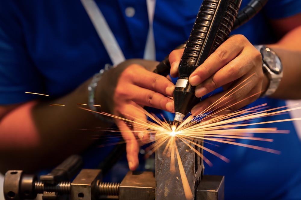
Here we discuss electro-spark deposition applied to metal alloys in order to repair defects in injection molding tooling and casting molds.

Image Credit: FUN FUN PHOTO/Shutterstock.com
What is Electro-Spark Deposition?
Electro-spark deposition (ESD) is used for the precision repair of high-value worn components on a small scale using pulse micro-welding. Electro-spark deposition is also known as pulsed electrode surfacing, pulsed fusion surfacing, electro-spark alloying, electro-spark toughening, and spark hardening. In industry, it is used for repairing defects in injection molding tooling and casting molds.
ESD systems have a capacitor-based power source producing pulses through a rotating wire consumable electrode. These pulses have a high current in a very short duration. The material of the consumable electrode (anode) deposits itself on the workpiece (cathode) through an electric spark.
ESD Applied to Metal Alloys
A high-temperature plasma arc is generated between the electrode’s tip and metal alloy workpiece by the direct current when the capacitor energy is released. This high temperature ranges between 8000 to 25000°C. The plasma arc ionizes the anode, and this molten material is then transferred onto the workpiece rapidly.
This ionized anode is transferred onto the substrate through short pulses. The high-temperature arc consists of anode particles, thermal flux (heat jet), and plasma (developed by gases decomposition and nitrogen, oxygen, and carbon active atoms). The major portion of heat is carried by the heat jet and the plasma.
Since the pulses are short, the heat transfer via heat jet and other gases is minimal, and the only heat transfer to the substrate is through the small number of anode microparticles deposited on the substrate. Therefore, these pulses impart a small heat input to the substrate, which results in no modifications of its microstructure. This method can be more beneficial than fusion welding processes generally used to repair alloys that have poor heat affected zone properties (like low toughness, high hardness, liquation cracking).
Furthermore, this process helps create a strong metallurgical bond between substrate and coating. Microalloying between electrode melt and base materials initiates the formation of plasma through air decomposition, carbonatites, carbides, and nitrides.
Discharge Parameters
The deposition quality depends on specific discharge parameters such as pulse time, current, and voltage, which rely on the chemical and physical properties of device-electrode-based materials. Therefore, the parameters depend on the electrode deposition type, temperature dependence, flowability, electrical resistance, density, diffusivity, chemical reactivity of anode elements, thermal conductivity, and melting temperatures.
Advantages
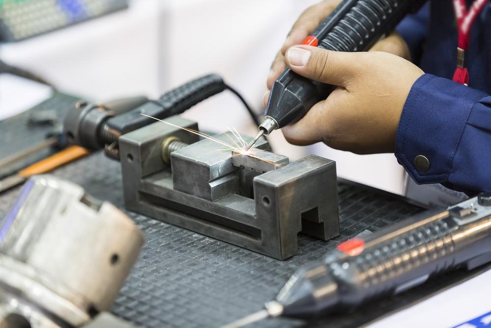
There are several advantages associated with ESD applied to metal alloys. For instance, no special preparation of the surface of the workpiece is required. The deposited layer attains amorphous specific properties due to high solidification speed, and it may not need subsequent finishing. ESD can be easily applied to the complex part’s surface, allowing deposition in strictly indicated places. Both metal alloys and pure metals can be used as an electrode. ESD allows the use of hard fusible compounds and metallic ceramics for deposition.

Image Credit: Aumm graphixphoto/Shutterstock.com
Another advantage of ESD applied to metal alloys is that there is a lack of heating of the sample in the process of deposition. In addition, ESD provides pollution-free procedures by eliminating the usage of poisonous nonmetallic materials like cyanide in the coating process. Moreover, the equipment is very simple, and the quality of the additive materials determines the costs associated with ESD.
A further advantage of the ESD procedure is that the heat density of the piece is very low, which helps maintain the properties of the basic material and its chemical composition. The thin layers formed by the ESD method are divided into two sub-layers. The interior diffused layer has the resultant properties of both basic and added material, whereas the surface or exterior layer has a strongly modified structure. ESD also increases the erosion and wear resistance of small surface areas.
Limitations
ESD is ideal for repairing shallow and minor defects; however, it is not suitable for large defects due to the slowness of the process and the maximum thickness of coating being 2mm.
Sometimes, the geometry of the substrate limits the coating. The contact between electrode and surface of the substrate is necessary for ESD, but some surface geometries do not allow such contact; therefore, the coating is only applied to adjacent areas.
The characteristics of deposited layers are governed by process parameters like pressure on the electrode tip, the number of passes over each area of substrate, temperature, frequency, spark duration, spark energy etc. Surface waviness with a period less than the diameter of the electrode can cause the coating to build only on the peaks. Some deposition parameters might cause initial covering to be insufficient, leaving some parts uncovered. As the arc goes to the closest surface, only the high points will continue to build up with successive passes and layers. The solution for this issue is choosing an optimum work regime through suitable parameters.
Recent Studies
Recently there has been a lot of research conducted on applying ESD simultaneously with other methods to make specific alloys. For example, in 2021, a paper was published by researchers at the University Politehnica of Bucharest, Romania, investigating a groundbreaking high corrosion-resistant coating deposited via ESD.
In this research, an alloy with high entropy was fabricated through the dust of Zr, Ti, Ta, Nb and Hf by mechanical alloying and spark plasma sintering. A thin layer was coated on a stainless steel sample through ESD. This coating had improved hardness compared to the substrate, and when they tested for corrosion resistance it showed a very low corrosion rate of 0.00024 mm/year.
More from AZoM: What is Cryo-Electron Microscopy?
References and Further Studies
Johnson, R. N. (2002). Alternative coatings for wear and corrosion: the electrospark deposition process. published in Proceedings, American Electroplaters and Surface Finishers Society. https://www.nmfrc.org/pdf/awk02/awk02d06.pdf
Manea, C. A., Sohaciu, M., Stefănoiu, R., Petrescu, M. I., Lungu, M. V., & Csaki, I. (2021). New HfNbTaTiZr High-Entropy Alloy Coatings Produced by Electro-spark Deposition with High Corrosion Resistance. Materials, 14(15), 4333. https://www.mdpi.com/1996-1944/14/15/4333
Twi-global, What is electro-spark deposition (ESD)?. [online] Available at: https://www.twi-global.com/
Vizureanu, P., Perju, M., & Nejneru, D. A. C. (2018). Advanced Electro-Spark Deposition Process on Metallic Alloys. In (Ed.), Advanced Surface Engineering Research. IntechOpen. https://www.intechopen.com/chapters/62514
Disclaimer: The views expressed here are those of the author expressed in their private capacity and do not necessarily represent the views of AZoM.com Limited T/A AZoNetwork the owner and operator of this website. This disclaimer forms part of the Terms and conditions of use of this website.