The development of organic light-emitting diode (OLED) visual display technologies harnesses the properties of two key techniques: photoluminescence and electroluminescence.
Confocal microscopy can be used in conjunction with both techniques to image the optoelectronic properties of an OLED device. This is made possible with the RMS1000 Confocal Raman Microscope.
Spectral and time-resolved imaging offers a more detailed insight regarding the composition and quality of the device when compared to bulk measurements.
Introduction
Today, organic light-emitting diodes (OLEDs) are among the leading technologies for full-color display panels used in premium smartphones and televisions.1 This rapid rise in OLED technology offers superior performance to liquid crystal displays (LCDs). For instance, they are more flexible, thinner, lighter, less power consumptive, and brighter than comparative technologies.2
In standard OLED devices, electrons and holes are introduced to organic electron and hole transport layers before recombining in a central doped emission layer. The energy generated by this recombination stage is transferred to a dopant molecule via resonant transfer, emitting light.
The chemical structure of the dopant molecule in the emission layer determines the color of the OLED emission. When new OLEDs are developed, photoluminescence (PL) and electroluminescence (EL) spectroscopy can characterize the optoelectronic properties of both individual components and the final product.
This article outlines how the RMS1000 Confocal Raman Microscope can be used to characterize and spatially resolve the optoelectronic properties of an OLED device leveraging four different imaging modalities: PL, EL, time-resolved PL (TRPL), and time-resolved EL (TREL). A confocal microscope offers greater detailing when characterizing an OLED's spectral and time-resolved properties compared to when using bulk measurements.
Materials and Methods
The Organic Semiconductor Optoelectronics group at the University of St Andrews prepared a phosphorescent OLED device for the purpose of this study. The sample was carefully centered on an electrical probe stage (LINKAM HFS350EV-PB4) and two tungsten probes were coupled with the device’s electrodes to illuminate a single OLED pixel. Using an RMS1000 Confocal Raman Microscope, as shown in Figure 1, spectral and time-resolved PL and EL imaging was conducted.
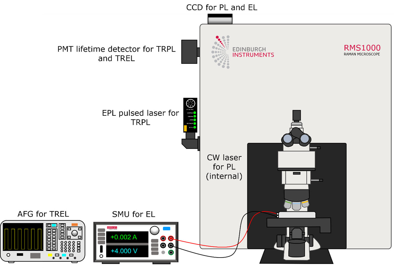
Figure 1. Experimental setup for PL, TRPL, EL, and TREL imaging. Image Credit: Edinburgh Instruments Ltd.
The sample was contained in the electrical probe stage and placed in the microscope stage insert, as demonstrated in Figure 2. To run spectral PL measurements, a 532 nm CW laser and a back-illuminated CCD camera was incorporated into the system.
For TRPL measurements, a combination of an externally coupled EPL-405 picosecond pulsed diode laser, phosphorescence lifetime electronics based on single photon counting multichannel scaling (MCS), and a High-Speed PMT lifetime detector were fitted to the system.
For spectral EL measurements, it was necessary to apply a bias to the OLED device and detect electroluminescence with the CCD using a Keithley 2450 Source Measurement Unit (SMU). Lastly, to conduct TREL measurements, a Tektronix 31102 Arbitrary Function Generator (AFG) was used to generate a train of short voltage pulses applied to the OLED. The decay that occurs after each pulse was determined using MCS.
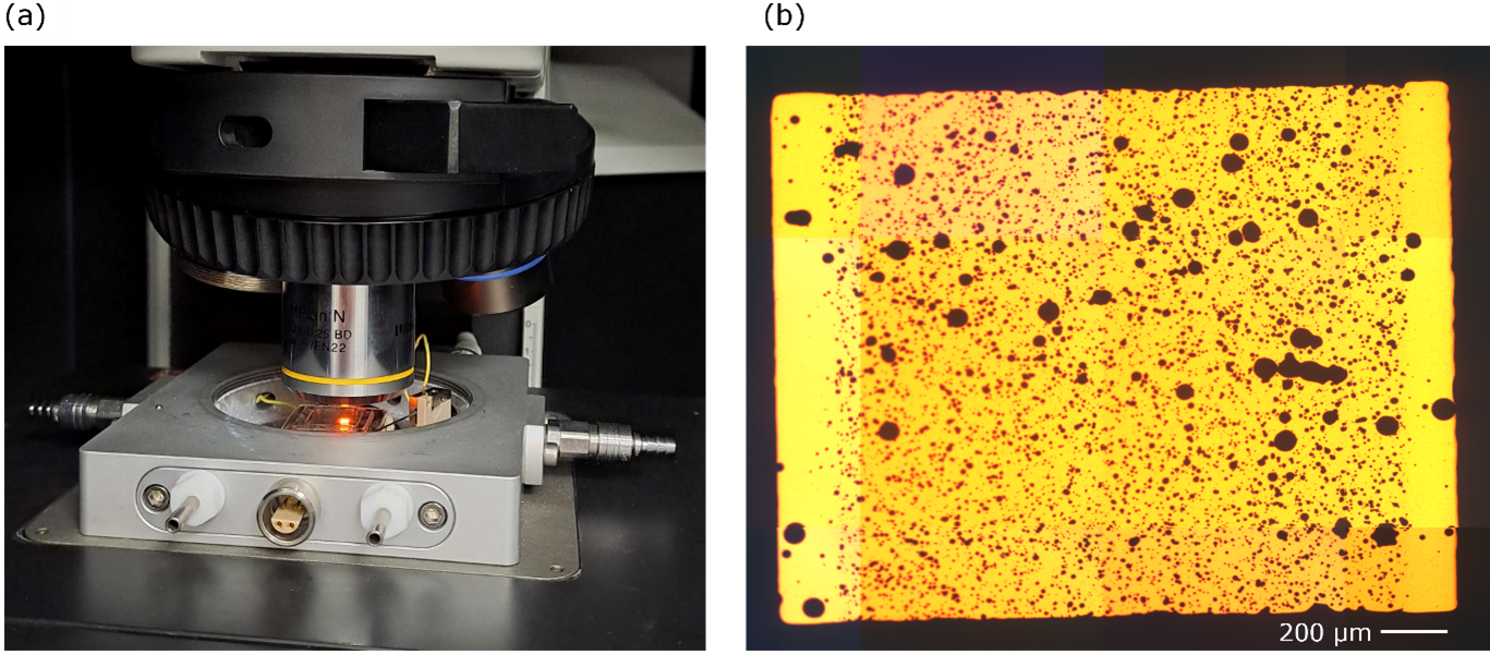
Figure 2. (a) Electrical probe stage fitted on the RMS1000. (b) Widefield view of electroluminescent OLED pixel through the microscope. Image Credit: Edinburgh Instruments Ltd.
Results and Discussion
Large Area Photoluminescence and Electroluminescence Spectral Imaging
The OLED was initially evaluated using a combination of spectral PL and EL. Using a confocal microscope, these techniques can be paired with imaging techniques to reveal information related to the distribution of the optically relevant materials throughout the device. Moreover, it is possible to acquire additional information regarding overall quality relating to the uniformity of the emission intensity and color throughout the device.
The PL image and relative spectra displayed in Figure 3 demonstrate the distribution of the emissive layer over a 4-pixel area on the device, and the location of the electrodes are displayed for reference.
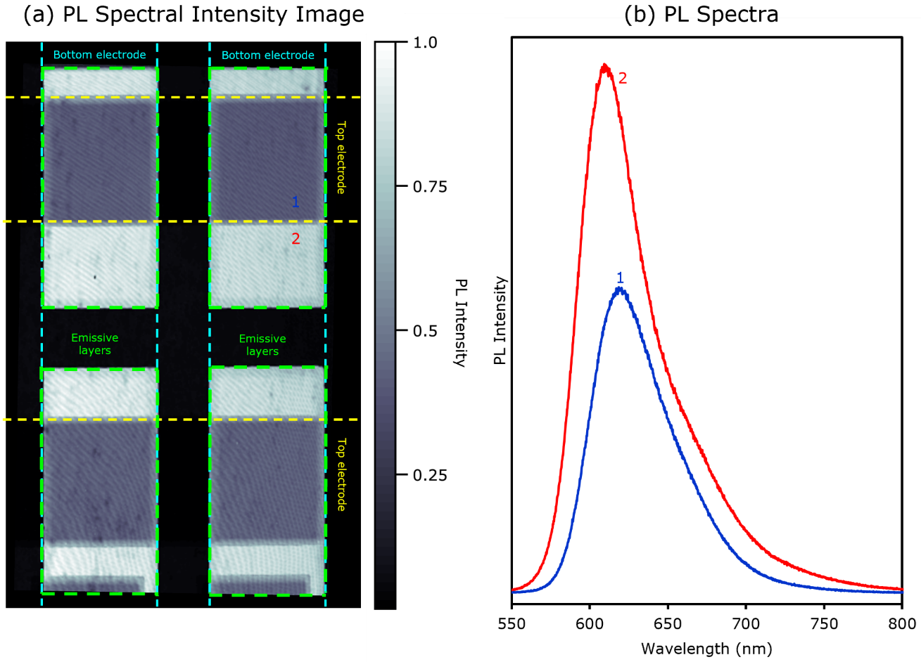
Figure 3. (a) Spectral PL image of OLED device. (b) PL spectra from points 1 and 2 are labeled in the image in (a). Image Credit: Edinburgh Instruments Ltd.
The white (high) and grey (low) PL intensity regions are grouped in the green border to present a visualization of the location of the organic emissive layers over the four pixels.
It was resolved that the grey regions represent the locations at which the top electrodes covered the emissive layer. This is because where the top electrode meets the emissive layer, there is a reduction in the PL emission which amounts to less than half the intensity of the uncovered areas. This is caused by the material of the top electrode material, which restricts the intensity of both the incoming laser and the outgoing PL.
For EL imaging, the probes were attached to electrodes that overlapped on Pixel 2. The EL image that was captured, as shown in Figure 4, reflects this alongside the corresponding spectra, with EL emission visible only in the region where the emissive layer in Pixel 2 intersected with the top and bottom electrodes.
With PL mapping, the spatial resolution is primarily influenced by the size of the laser spot to which the sample is subjected. In the EL image, no excitation laser is present to offer any spatial resolution. Rather, for EL, the confocal pinhole diameter was leveraged to generate the spatial resolution by adjusting the pinhole diameter to its smallest possible setting of 25 μm.
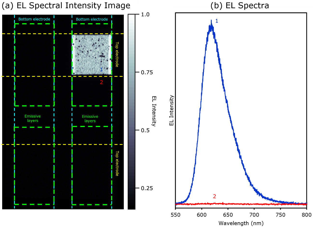
Figure 4. (a) Spectral EL image of OLED device. (b) EL spectra from points 1 and 2 labeled in the image in (a). Image Credit: Edinburgh Instruments Ltd.
Across the active pixel, the EL intensity is uneven, impacting the device's overall quality. Two vertical strips at the outer edges (white) of the emitting pixel produce more EL than the rest of the pixel. Moreover, there are several non-emissive regions in the pixel where the EL intensity is limited. This suggests that there are defective regions in the pixel. Ideally, an OLED should exhibit intense, uniform emissions across each pixel.
High-Resolution Photoluminescence and Electroluminescence Spectral Imaging
To further evaluate the aforementioned effects observed in the PL and EL maps, a more concentrated region of the EL active pixel was imaged using PL and EL techniques, as shown in Figures 5a and 5b. The upper region of the mapping grid shows where the emissive layer overlapped with the electrodes, and the lower region is where the emissive layer was observed in isolation.
The PL intensity image (Figure 5c) demonstrates how the top electrode limits the intensity of the incoming laser and outgoing PL light, as the observed intensity from the isolated emissive layer is greater than the layer which intersects with the electrodes.
The PL peak wavelength image (Figure 5d) demonstrates how, within the EL active electrode-covered emissive layer, the PL emission is red-shifted (620 nm) in contrast to the uncovered emissive layer region (611 nm). This difference in peak wavelength suggests that different energy levels are being accessed in different regions.
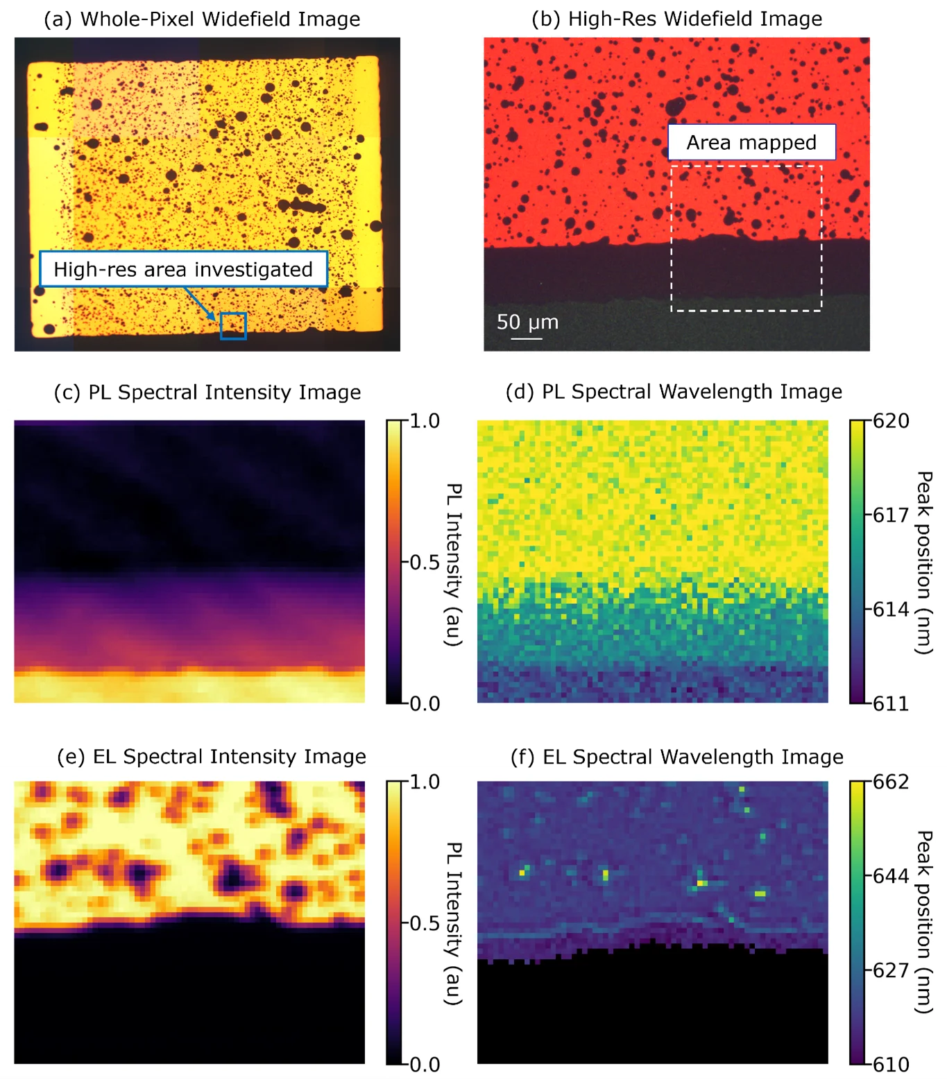
Figure 5. (a) Whole-pixel and (b) high-resolution widefield images of electroluminescent OLED pixel. (c) PL intensity and (d) peak wavelength images of the EL boundary of the OLED pixel. (e) EL intensity and (f) peak wavelength images of the same area. Image Credit: Edinburgh Instruments Ltd.
The EL imaging indicates that the pixel with less emissive defects in the pixel (Figure 5e) has a large redshift (Figure 4f) when contrasted with the rest of the pixel. This is a consequence of the intensity decrease in the EL band observed across the rest of the pixel and the parallel increase in a second, lower energy EL band at 662 nm.
In addition, a blue shift can be observed in the region at the very bottom of the EL active region in Figure 3. This is consistent with the change in wavelength determined across the PL image. Each of these observations, which were captured with high-resolution spectral imaging, reveal significantly higher levels of complexity than could be observed using bulk PL and EL measurements.
High-Resolution Time-Resolved Photoluminescence and Electroluminescence Imaging
TRPL and TREL imaging were conducted across the same area to acquire more information, as shown in Figure 6. Here, the sample was exposed to laser and electrical pulses for PL and EL, respectively, and PL and EL lifetime decays of the OLED were documented at 614 nm in MCS mode. A single exponential decay model was applied to the decays to extract the lifetime.
In the TRPL image (Figure 5a), the PL lifetime throughout the EL active region (upper region) was around 200 ns shorter than the PL lifetime within the EL inactive region (lower region). The longest and shortest lifetimes documented were recorded at 800 ns and 600 ns, respectively (Figure 5b).
A gradient was detected similar to the PL intensity and wavelength images, as exhibited in Figure 4. Here, a reduction in emission intensity can be seen down the map and a blue shift occurs. Therefore, the TRPL data concludes that, when excited optically, a range of energy levels are accessed across the dopant strip. In the TREL image (Figure 5b), the lifetime across the entire region is similar at around 470 ns. The EL lifetime was considerably shorter than the PL lifetime recorded across the same area.
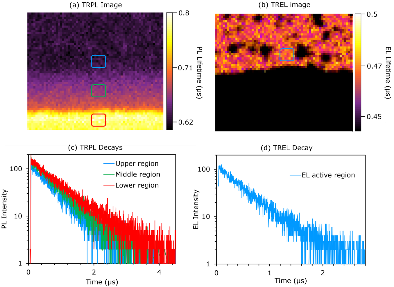
Figure 6. (a) Time-resolved PL image of OLED pixel. (b) Time-resolved EL image of OLED pixel. (c) PL lifetime decays from the image in (a). (d) EL lifetime decay from the image in (b). Image Credit: Edinburgh Instruments Ltd.
Conclusion
To successfully conduct PL, EL, TRPL, and TREL imaging of an OLED device, the RMS1000 Confocal Raman Microscope was used for this study.
Overall, the various imaging modes used generated a wealth of key information related to the efficiency and color uniformity of a pixel within the device under working conditions. Furthermore, it was possible to place the location of the emissive layer and electrodes throughout the device and gain vital information that revealed the energy levels during the two imaging processes.
Acknowledgments
We would like to thank the Organic Semiconductor Optoelectronics group at the University of St Andrews for providing the OLED described in this study.
References and Further Reading
- A. Salehi et al., Recent Advances in OLED Optical Design, Adv. Funct. Mater., 2019, 29, 1808803, DOI: 10.1002/adfm.201808803.
- J. M. Ha et al., Recent Advances in Organic Luminescent Materials with Narrowband Emission, NPG Asia Mater., 2021, 13, 1–36, DOI: 10.1038/s41427-021-00318-8.
- T. Deksnys et al., Synthesis and Characterisation of a Carbazole-Based Bipolar Exciplex-Forming Compound for Efficient and Color-Tunable OLEDs, New J. Chem., 2017, 41, 559–568, DOI: 10.1039/C6NJ02865A

This information has been sourced, reviewed and adapted from materials provided by Edinburgh Instruments Ltd.
For more information on this source, please visit Edinburgh Instruments Ltd.