4D STEM is currently used in many TEM projects and is for sure on every electron microscopist’s “must-watch” list. Recent advancements in TEM technology, particularly the hybrid-pixel direct electron detector, have contributed to its widespread use in Materials Science.
Regardless of naming protocols or its diffraction mapping origin, 4D STEM is now the leading method for improving (virtual) STEM imaging, disclosing hidden electromagnetic fields, crystallography, and localized defects. It has also set new records for resolution through ptychography reconstructions.
STEM imaging involves rastering a high-energy electron beam across a thin sample and monitoring “selected” electrons that pass through it. The precise selection and identification of transmitted electrons yield high-resolution images with useful information for sample characterization.
Electrons scattered at high angles (>80 mrad) provide chemical (Z-) contrast, while electrons scattered at intermediate angles (within diffraction angles as determined by the sample’s crystalline structure) enhance the visibility of crystalline domains.
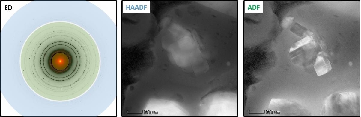
Figure 1. (left) The diffraction pattern of a polycrystalline Aluminum sample with the most common STEM detector overlays – HAADF (blue), ADF (green), and BF (yellow). (center, right) STEM imaging of Aluminum Oxide precipitates, as achieved with different detectors and detection regions. These images evidence chemical contrast and crystal grain contours. Image Credit: Dectris Ltd
In addition to the features that may be observed directly with traditional STEM imaging, a far more precise view of TEM samples can be obtained using comprehensive electron scattering distribution (or diffraction pattern) analysis.
For example, diffraction patterns in TEM can be used to obtain exact measurements of local electromagnetic fields and details of a sample’s crystalline structure and defects (similar to EBSD maps on SEMs).
![(left) A survey of a 4D STEM experiment on a CoNi nanowire [1]. (center) The sum of diffraction patterns within the 4D STEM dataset, acquired a Gatan Stela camera (hybrid-pixel DECTRIS ELA detector integrated into DigitalMicrograph software for advanced electron diffraction experiments) [2]. The dashed lines indicate virtual detector locations for virtual STEM images. The diffraction pattern indexing indicates a Ni cubic structure oriented along the [110] zone axis. (right) Virtual STEM images, as reconstructed in DigitalMicrograph software from the 4D STEM dataset. These evidence the nanowire’s morphology (BF), bend contours (DFg), and the presence of a sub-grain (DF’).](https://www.azom.com/images/Article_Images/ImageForArticle_23592_17138447600912768.png)
Figure 2. (left) A survey of a 4D STEM experiment on a CoNi nanowire 1. (center) The sum of diffraction patterns within the 4D STEM dataset, acquired with a Gatan Stela camera (hybrid-pixel DECTRIS ELA detector integrated into DigitalMicrograph software for advanced electron diffraction experiments) 2. The dashed lines indicate virtual detector locations for virtual STEM images. The diffraction pattern indexing indicates a Ni cubic structure oriented along the [110] zone axis. (right) Virtual STEM images, as reconstructed in DigitalMicrograph software from the 4D STEM dataset. These evidence the nanowire’s morphology (BF), bend contours (DFg), and the presence of a sub-grain (DF’). Image Credit: Dectris Ltd
For years, TEM users have decoded the properties of samples from recorded diffraction patterns, while some more enthusiastic professionals have tried scanning a small electron beam over a region of interest to capture localized diffraction patterns as a map.
Regardless of their limited success (Spoiler: their detector technology was a primary constraint!), their efforts are identical to today’s widely accepted 4D STEM3 practice of recording a 2D array of electron probe positions, each containing a (2D) localized diffraction pattern captured with a pixelated detector.
4D STEM, whether new or rebranded, has recently emerged as a prominent topic in nanoscale materials characterization.
Recording Diffraction Patterns in STEM
STEM imaging with multiple annular detectors is useful for capturing and combining scattering data from delimited regions of a diffraction pattern.
The detectors operate as a “one-pixel camera” by returning the overall electron count (as a gray level) from the collection zone. This enables an exceptionally fast time per pixel (also termed “dwell time”), often in the µs range.
For example, recording a standard STEM image with a 1024 x 1024 scan array and a dwell time of 5 µs only takes about 5 seconds. However, integrating signals by STEM detectors yields less information than the ideal recording of entire diffraction patterns as 2D images.
The evolution of electron recording detectors (which skipped the photographic plates for practical reasons) significantly enhanced the acquisition speed for images and diffraction patterns.
The transition from CCDs to CMOS detector design enabled TEM cameras to reduce their acquisition time from approximately 1 second to a few milliseconds for a 512 x 512 pixel image.
Despite this significant speed-up, 4D STEM investigations remained out of reach: the same 1024 x 1024 scan array, now with a dwell time of 3.3 ms, would take around 55 minutes to complete.
This impractical experiment may result in a distorted dataset because of sample drift or an “unhappy” sample from a high electron dose.
A potential compromise on 4D STEM data acquisition with ordinary CMOS cameras is to decrease the scan array (to 128 x 128 points, for example) to enable faster acquisitions (around one minute). However, this would result in the loss of spatial resolution and/or field of view for the measurement.
The Latest Detectors and “5D STEM”
The recent development of hybrid-pixel technology for electron detection is rapidly altering perspectives on 4D STEM studies. In addition to significantly improving the acquisition speed of TEM images and diffraction patterns, hybrid-pixel direct electron detectors possess better sensitivity.
This enhanced ability can distinguish single-electron events and has a wider dynamic range, allowing more flexible diffraction experiments.
DECTRIS hybrid-pixel detectors can function at 4500 Hz (with an 8-bit dynamic range and a readout of 1024 x 512 pixels for DECTRIS ELA detectors), resulting in a full diffraction pattern every 220 µs.
The aforementioned 4D STEM experiment (with a 1024 x 1024 scan array frame) now takes about 4 minutes. This is appropriate even for atomically resolved maps, as modern TEM microscope drift rates are well below 0.5 nm/minute.
If faster acquisitions are required, speeds of up to 18,000 Hz can be easily achieved by using a smaller detector region for readout.
Aside from acquisition speed (which is the scope of this article), hybrid-pixel detector efficiency (DQE) impacts the quality of the recorded diffraction patterns.
It is safe to say that the higher acquisition speeds, combined with moderate beam currents (considering potential sample damage), will result in fewer electrons per electron diffraction snapshot, with a maximum of few counts for most pixels.
In this scenario, DECTRIS hybrid-pixel technology enables noise-free acquisition with single-electron sensitivity, making it ideal for recording fast 4D STEM datasets. Time-resolved 4D STEM, sometimes known as “5D STEM” with the addition of time as a dimension, is also emerging as a novel approach.
At the current maximum speed, acquiring a 128 x 128 scan array takes less than a second, and the new generation of detectors is not slowing down. Users can fine-tune data analysis algorithms, as complete diffraction patterns will flow in.
References and Acknowledgments
- Sample provided courtesy of Cristina Bran, Institute of Materials Science Madrid (ICMM-CSIC)
- Liam Spillane and Ana Pakzad’s (AMETEK, Gatan) support during experiments and discussions is greatly appreciated.
- B. Plotkin-Swing et al., Ultramicroscopy (2020), DOI: 10.1016/j.ultramic.2020.113067

This information has been sourced, reviewed and adapted from materials provided by Dectris Ltd.
For more information on this source, please visit Dectris Ltd.