Building an integrated circuit (IC) requires various physical and chemical processes to be performed on a semiconductor (e.g., silicon) substrate. Millions of transistors can be fabricated and wired together by producing structures of different components to make up the sophisticated circuitry needed in a contemporary microelectronic device. The key to these processes is lithography.
Optical lithography is a photographic procedure in which a light-sensitive polymer, known as a photoresist, is exposed and developed to generate 3D relief images on a substrate. Typically, the optimal photoresist image has the precise shape of the designed or intended pattern in the substrate’s plane, with vertical walls through the thickness of the resist.
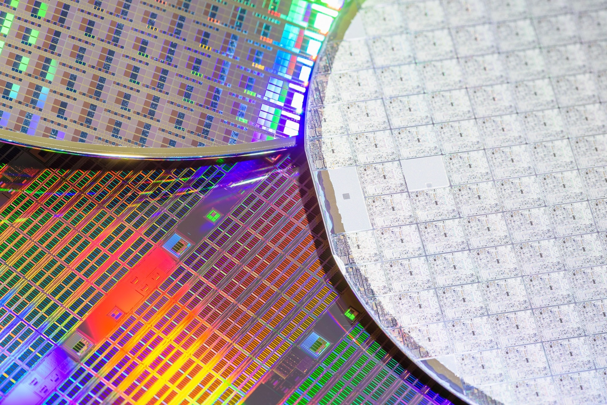
Image Credit: William Potter/Shutterstock.com
The final resist pattern is thus binary: some substrate components are covered with resist while others are left entirely uncovered. This binary pattern is required for pattern transfer as the substrate's parts covered with resist are protected from etching, ion implantation, and various other pattern transfer mechanisms.
The usual sequence for a regular optical lithography procedure is below:
- Substrate preparation
- Photoresist spin coat
- Prebake, exposure
- Post-exposure bake
- Development
- Post bake
Lithography, being optimized for IC technology, possesses a strong 2D nature. This is because the IC fabrication process flow consists of stacking multiple virtually two-dimensional high-precision process layers. The layout of each layer is built considering both XY positions and dimensions, characterizing areas that are either opaque or transparent.
Comprehensive data on the homogeneity of the photoresist layer deposited on a wafer is needed for certain process control and optimization aspects.
Assessing the thickness and homogeneity of photoresists, which can measure up to several hundred micrometers in thickness, presents a significant challenge for most non-contact optical approaches.
Equipped with a wide range of interferometric sensors, MicroProf® provides the ideal solution for measuring photoresist thicknesses. It utilizes interferometric sensors for extremely accurate, spatially resolved coating thickness assessments.
Clients have an extremely dynamic measuring system for rapid, spatially resolved layer thickness and topography assessments in a multi-sensor arrangement with an interferometric measuring head and a confocal chromatic topography sensor. With MicroProf®, it is possible to carry out high-resolution 3D measurements of the homogeneity of the photoresist on wafers up to 300 mm.
The wafer is recorded fast and non-destructively. The degree of automation spans from manually operated measuring systems like the MicroProf® 300, which spontaneously execute predefined programs, to fully automated wafer handling, such as automatic pre-alignment and fine alignment in the MicroProf® AP.
Overlay, which results from an alignment-exposure-development procedure, is among the fundamental benchmarks for a lithographic procedure. Accurate overlay characterization demands vast quantities of assessments over the wafer, which is why instruments for overlay measurement are typically automated.
The measurement principle of optical overlay assessments depends on pattern recognition of customized features. This means that alignment performance relies on the optical quality of the marker images.
A specialized software package for Acquire Automation XT provides fully automated assessment and analysis of the overlay offset in the x- and y-direction alongside the microstructure rotation.
Whether for laboratory, development, quality assurance, or production, Camtek FRT Metrology delivers superb measurement technology for applications from Advanced Packaging.

This information has been sourced, reviewed and adapted from materials provided by Camtek FRT Metrology.
For more information on this source, please visit Camtek FRT Metrology.