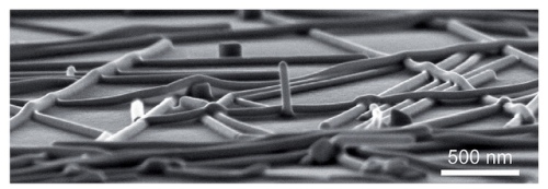
A Stanford University research team has developed a novel technique based on the physics of plasmonics to weld nanowires using a simple light blast, paving the way to develop easy and large-area processing methods for electronic devices such as LEDs, thin-film solar cells and touch-screen displays.
 This titled, cross-sectional scanning electron microscope image shows nanowires of silver that have been welded together by in a new technique developed at Stanford. (credit: Mark Brongersma, Stanford University)
Mark Brongersma, one of the researchers, explained that it is a known fact that plasmon waves will be generated by light at the meeting place of two nanowires when they are laid crisscrossed, resulting in the formation of a hot spot. It is a self-limiting process that stops welding by itself, because these hot spots exist only while the nanowires are in contact but not after their fusion.
According to Michael McGehee, one of the researchers, another important advantage of the process is that it does not affect the remaining wires as well as the underlying material. This accurate heating capability significantly improves the energy efficacy, speed and control of nanoscale welding.
In this technique, when individual nanowires that are laid atop each other are illuminated, the top nanowire behaves like a tiny antenna that directs the light’s plasmon waves into the bottom wire and generates heat to weld the wires. Besides easily fabricating high-performance and stronger nanowire meshes, the novel technique paves the way to produce mesh electrodes bound to transparent or flexible polymers and plastics.
To illustrate the capabilities of this technique, the research team applied a mesh over a saran wrap. The team sprayed and dried a suspension comprising silver nanowires on the plastic and then illuminated. The resulting product was an ultrathin welded nanowire layer. The layer is almost transparent when it is held up like a paper and retains its electrical properties when it is unfolded, informed Yi Cui, one of the researchers.