A research team from Georgia Tech supported by the National Science Foundation has developed a novel technique termed as magnetically actuated peel test (MAPT) in order to determine the adhesion strength between thin material films that find applications in MEMS, photovoltaic cells and microelectronic devices. The research was published in the March 30, 2012 issue of the Thin Solid Films journal.
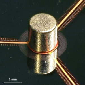
 Image shows an assembled magnetically actuated peel test (MAPT) specimen being prepared for analysis at the Georgia Institute of Technology. The silver cylinder in the center is the permanent magnet.
MAPT is a non-contact and fixtureless technique that enables electronic devices to be consistent over the long-term and help designers enhance resistance to mechanical and thermal stresses.
Doctoral student Gregory Ostrowicki and professor Sitaraman were successful in determining the adhesion strength between silicon dioxide insulator and copper conductor layers. This technique can also be used to study fatigue cycling failure, which takes place over a period of time especially because the interface between layers is subjected to stress continuously. The technique may also be utilized to study adhesion between layers in MEMS devices and photovoltaic systems.
Initially Georgia Tech researchers utilized standard microelectronic fabrication techniques to form thin film layers that needed to be studied on a silicon wafer. At the sample center, a small nickel-plated neodymium (NdFeB) permanent magnet was linked to three thin-film copper grown atop silicon dioxide ribbons on a silicon wafer.
The sample was next mounted between an optical profiler and an electromagnet in a test station. Voltage applied to the electromagnet was gradually increased over time, resulting in a repulsive force between the like magnetic poles. The upward pull by the permanent magnet’s repulsive force caused the copper ribbons to stretch until they finally delaminated.
The magnetic field strength and data from the optical profiler enabled the researchers to offer a precise measure of the force needed for sample delamination. Since it is possible to make a large number of samples simultaneously on the same wafer, large volume of adhesion data can be obtained in time.
Sitaraman and Ostrowicki have conducted research on thin film layers about 1 µm thickness, but are confident that this technique will also work on sub-micron layers.