Oct 7 2014
A research team from the University of Southampton have invented an innovative method of using silicon detectors in the field of telecommunications.
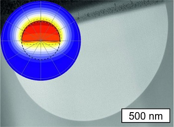
 This is a single-crystal-like silicon core fiber with a thermodynamic snap shot of the laser heating. Credit: University of Southampton.
Silicon has been seen as a promising material in microelectronics industry for several years, due to its exceptional optical properties in the near and mid infrared region. Due to these properties, the material is now found to be ideal for photonics applications too.
The research involves resolving the limitations of silicon’s application in telecommunications by altering the electronic band structure within the laser-crystallized silicon photonic devices.
The team developed a laser processing technique suitable for fabricating silicon optical fibre. The process explains the possibilities of thoroughly crystallising the core material, adjusting the optoelectronic properties and attaining reductions in bandgap from 1.11eV to 0.59eV to facilitate optical detection at 2100nm.
Using silicon materials eliminates the difficulties when coupling the nanoscale waveguides on-chip used for data processing, communications systems and micron-sized fibres for light transportation.
According to the research team, the process of creating single crystal-like materials within the fibre core opens the door to the possibility of developing silicon fibre devices with optoelectronic properties.
The utilisation of a wide range of variable strains has offered excellent control of optoelectronic properties of silicon thereby increasing the chances of using silicon in optical and electrical devices.
This research has demonstrated the ability to split the band gap energy of silicon, allowing it to serve as an optical detection medium in the telecommunications band. The team at the University of Southampton believe that this breakthrough laser processing technique can be applied to a large number of material systems.