Apr 10 2019
With the improved power of the new measuring method that can characterize materials at scales considerably smaller than any existing technologies, the discovery and study of 2D, micro- and nanoscale materials can be accelerated.
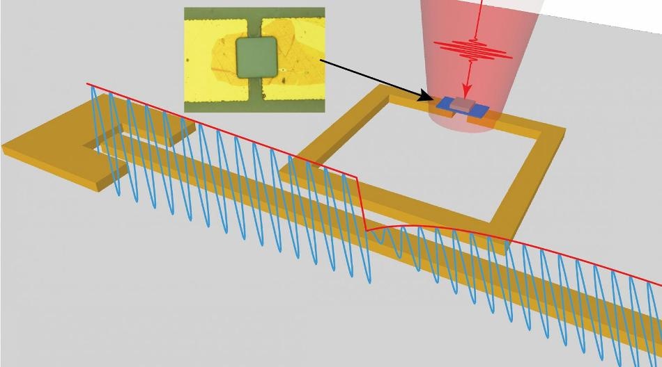
 Rendering of microwave resonator showing the (blue) microwave signal’s size change resulting from a light pulse (red) once the pulse hits the infrared pixel (micrograph image of the pixel is shown in the inset). (Image credit: UT Cockrell School of Engineering)
The ability to precisely determine semiconductor properties of materials in small volumes enables engineers to determine the range of applications for which these materials may be appropriate in the future, specifically since the size of optical and electronic devices continues to decrease.
Daniel Wasserman, an associate professor in the Department of Electrical and Computer Engineering in the Cockrell School of Engineering, headed the team that developed the physical system, created the measurement method that can obtain this level of sensitivity, and successfully presented its enhanced performance. Their study was published on April 9th, 2019 in Nature Communications.
The design approach of the team was focused on creating the potential to give quantitative feedback on material quality, with specific applications for the growth and manufacturing of optoelectronic devices. The technique presented has the ability to measure many of the materials that engineers hope will someday be omnipresent to next-generation optoelectronic devices.
Optoelectronics refers to the study and application of electronic devices that are able to source, detect, and control light. Optoelectronic devices that detect light, called photodetectors, employ materials that produce electrical signals from light. Photodetectors are present in solar cells, smartphone cameras, and in the fiber optic communication systems that constitute the broadband networks. In an optoelectronic material, the amount of time that the electrons continue to be “photoexcited,” or the ability to produce an electrical signal, is a reliable indicator of the potential quality of that material for photodetection applications.
The existing technique used for measuring the lifetimes or carrier dynamics of photoexcited electrons is expensive and complicated and only quantifies large-scale material samples with restricted accuracy. The UT team decided to try another technique for measuring these lifetimes by keeping small volumes of the materials in uniquely designed microwave resonator circuits. Samples are subjected to focused microwave fields while inside the resonator. On irradiating the sample with light, the microwave circuit signal changes, and the variation in the circuit can be measured on a standard oscilloscope. The decay of the microwave signal denotes the lifetimes of photoexcited charge carriers in small volumes of the material kept in the circuit.
Measuring the decay of the electrical (microwave) signal allows us to measure the materials’ carrier lifetime with far greater accuracy. We have discovered it to be a simpler, cheaper and more effective method than current approaches.
Daniel Wasserman, Associate Professor, Department of Electrical and Computer Engineering, Cockrell School of Engineering
Carrier lifetime is an important material parameter that offers insights into the whole optical quality of material while also determining the range of applications for which the material could be used when it is coupled into a photodetector device structure. For instance, materials with a very long carrier lifetime may be of high optical quality and thus very sensitive, yet may not be practical for applications that need high-speed.
“Despite the importance of carrier lifetime, there are not many, if any, contact-free options for characterizing small-area materials such as infrared pixels or 2D materials, which have gained popularity and technological importance in recent years,” stated Wasserman.
Infrared detection is one field that will definitely benefit from the real-world applications of this technology. Infrared detection is an important component in thermal imaging, molecular sensing, and some defense and security systems.
A better understanding of infrared materials could lead to innovations in night-vision goggles or infrared spectroscopy and sensing systems.
Daniel Wasserman, Associate Professor, Department of Electrical and Computer Engineering, Cockrell School of Engineering
High-speed detectors operating at these frequencies could even allow the development of free-space communication in the long-wavelength infrared—a technology enabling wireless communication in challenging situations, for example, in space or between buildings in urban environments.
The study was funded by Air Force Research Laboratories and is part of an ongoing partnership between Wasserman and his Mid-IR Photonics Group at UT, close collaborators at Eglin Air Force Base and scientists from The Ohio State University, University of Wisconsin, and Sandia National Laboratories.