Jun 14 2019
Using optical and electrical measurements, a two-dimensional anisotropic crystal of rhenium disulfide was found to show opposite piezoresistant effects along two principle axes, i.e. positive along one axis and negative along another. Piezoresistance was also reversible; it appeared upon application of a strain, but the relative resistance returned to its original value on strain removal. This novel finding is expected to lead to wide application of rhenium disulfide.
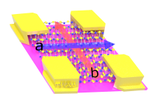
 Figure 1. Schematic of a ReS2 device on a flexible PI substrate, the channels of which are along the two principle axes of the ReS2 flake, respectively. ReS2 flakes were mechanically exfoliated from bulk crystals and transferred onto a flexible polyimide substrate. Two optical fibers were transferred onto the flake, each of which was perpendicular to one of the anisotropic axes of ReS2, respectively. Next, titanium/gold (Ti/Au) electrodes were deposited, followed by an optical filer lift-off process. Finally, Ag wires were connected to the electrodes for measurements.
Upon application of mechanical stress such as pressure on crystals and some kinds of ceramics, a surface charge proportional to the applied strain is induced; this phenomenon is called the piezoelectric effect. The piezoelectric effect has been known since the mid-18th century and has found use, for example, in the ignition device of cigarette lighters. Today it is widely applied in sensors, actuators, etc. On the other hand, when mechanical strain is applied to semiconducting materials, some of them show a change in electrical resistance, called the piezoresistive effect. Materials showing the piezoresistive effect are used in pressure sensors, strain sensors etc.
Rhenium disulfide (ReS2) is a two-dimensional (2D) material crystallizing into a flake-like structure, as a black platelet (plate-like crystal), showing thickness-independent direct bandgap*1) and anisotropic physical properties. It is classified into the transition metal dichalcogenides*2) subgroup. According to theoretical calculations, it has two anisotropic directions along different principle axes. Two anisotropic directions are predicted to respond differently to a uniaxial strain. Upon validation of this property, ReS2 should be useful in the accurate detection and recognition of multidimensional strain/stress and gestures, which will have wide applications in the fields of electronic skin*3), human‒machine interfaces, strain sensors etc.
This international research team from China and Japan, in which Dr. Liu from Tianjin University and Dr. Yang from WPI-NanoLSI, Kanazawa University, played important roles, not only confirmed the anisotropic piezoresistive effect of rhenium disulfide but also discovered a novel phenomenon that, depending on the direction of strain applied along two crystalline axes, a 2D device of ReS2 showed opposite, i.e. positive and negative piezoresistance.
A 2D device of ReS2 was fabricated as schematically depicted in Figure 1. After examining its configuration using atomic force microscopy (AFM), anisotropic properties were investigated by both optical and electrical methods.
First, optical measurements were performed using reflectance difference microscopy*4) (RDM) developed by the present research team. A device of ReS2 with an 8 nm thickness was irradiated with polarized light from various directions to determine the two axial (principle) directions of the 2D crystal (Figure 2).

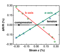
Figure 2. Relative resistance changes of the device along two axes as a function of strain. It shows the relative resistance change of this ReS2 device along the a- and b-axes, respectively, as a function of the strain. As expected, the a/b-axis showed positive/negative piezoresistance and almost linear change with the strain.
Next, electric anisotropy was measured with the same sample for optical measurements along 12 directions with a spacing of 30 degrees. These measurements also determined the two principle directions which showed a 110 degree difference. The same measurements were carried out with another device of ReS2, but with a different thickness (70 nm). The latter also yielded very similar anisotropic behavior, indicating the thickness-independent nature of the phenomenon. These results are consistent with previous work.
The 2D crystal ReS2 device whose principle axes were determined as above was clamped at one end along a principle axis and the other end was moved towards the fixed end at a specified speed, i.e. a compressive strain was applied. The device generated piezoresistance due to the strain. With one end fixed, piezoresistance recovered completely when the compressive strain of the other end was returned to its original state.
On the other hand, when the same experiment was performed along the other principle axis, the piezoresistance due to the strain was smaller when a larger strain was applied and increased when the applied strain was smaller. The same experiment was repeated with different ReS2 devices, but the results were always consistent. Thus, ReS2 2D crystalline devices showed opposite, i.e. positive or negative piezoresistance depending on the principle axes.
In addition, when the same experiment using a single device was repeated 28 times, almost the same results were obtained. This indicates that after applying a strain to the ReS2 device, releasing the strain allowed the piezoresistant effect to return to its original state.
While the piezoresistant effect is a result of the bandgap adjustment induced by a strain, the piezoelectric effect is a result of a strain-dependent distortion of the crystal lattice. Various electrical measurements were performed, which also demonstrated that the phenomenon observed was piezoresistance and not the piezoelectric effect.
The present study demonstrated that the ReS2 2D devices showed opposite, i.e. positive and negative piezoresistance depending on the principle axes along which a strain was applied. Such positive and negative piezoresistant effects depending on the principle axes were not observed in previous studies. Thus, the present study is the first to identify such an effect. It is expected that this study will lead to wide applications of ReS2 to electronics, such as electronic skin, human‒machine interfaces, strain sensors and so on.
Title: The Opposite Anisotropic Piezoresistive Effect of ReS2
Authors: Chunhua AN, Zhihao XU, Wanfu SHEN, Rongjie ZHANG, Zhaoyang SUN, Shuijing TANG, Yun-Feng XIAO, Daihua ZHANG, Dong SUN, Xiaodong HU, Chunguang HU, Lei YANG, and Jing LIU
Journal: ACS Nano 2019, 13, 3310−3319
Published online on March 6, 2019
DOI: 10.1021/acsnano.8b09161
URL: https://pubs.acs.org/doi/10.1021/acsnano.8b09161
[Glossary]
*1) Direct bandgap
The bandgap of a semiconductor is an energy range, between the valence band and the conduction band, where no electron states can exist. Direct band gap is a band gap in which the bottom of the conduction band and the top of the valence band exist on the same wave vector.
*2) Transition metal dichalcogenide
A chalcogenide is a chemical compound consisting of at least one chalcogen (oxygen family member including sulfur) anion and at least one more electropositive element. ReS2 has two sulfur atoms bonded to a Re atom, a transition metal. Since the molecule has two sulfur atoms, it is called dichalcogenide.
*3) Electronic skin
Electronic skin refers to flexible, stretchable and self-healing electronics that are able to mimic functionalities of human or animal skin, such as being capable to respond to environmental factors like changes in heat and pressure.
*4) Reflectance difference microscopy
Reflectance difference microscopy (RDM) measures the difference in reflectance of two beams of light with different linear polarization. The present international research team has developed the equipment used in this study.