Contact profilometry was likely one of the first techniques designed for measuring the roughness of a material’s surface by physically making contact with a surface or surface forces.
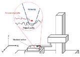
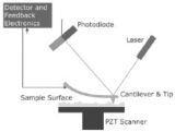
Stylus profilometers equipped with a diamond-tipped probe are the most common contact profilometers. Atomic force microscopy (AFM) uses the same concept for operation, but on a much smaller scale.
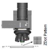
Novel measurement techniques that can perform measurements without making contact with the material surface are preferred in advanced systems and processes. Zeta-20 Optical Profilers are an innovative system from KLA, featuring ZDot™technology. The versatility, excellent cost of ownership, and speed of the Zeta-20 Optical Profiler make it an ideal replacement for the traditional stylus profilers in various applications.
Comparison of Stylus Profiler, AFM and ZDot™ Technology
The following table compares the capabilities of ZDot™ technology with the stylus profiler and AFM:
| |
 |
 |
 |
| Measurements |
Stylus Profiler |
AFM |
ZDot™ |
| Line scan roughness |
Yes |
Yes |
Yes |
| Line scan step height |
Yes |
Yes |
Yes |
| Area-based roughness and step height |
Slow (must combine multiple line scans) |
Slow (must combine multiple line scans) |
Fast |
| Large area measurements |
Slow, Minutes to Hours |
NO |
Fast, Seconds |
| Thinfilm thickness measurement |
Requires a film edge |
Requires a film edge |
Option for transparent films; no edge required |
| Characterization of buried surfaces |
No |
No |
Yes (if top layer is transparent) |
| True color or False Color |
False Color |
False Color |
True and False Color |
| Simultaneous 2D and 3D Analysis |
No |
No |
Yes (cross sections + area roughness) |
| Method and Limitations |
| Contact (does the sample get ‘touched’ by a probe?) |
Contact |
Contact |
Non-contact
Non-destructive |
| Artifacts (false readings) due to size of the probe? |
Yes, stylus shape and size can affect measurements; knowledge of the sample, the tip and some
Experience is all needed to identify artifacts. |
 |
No probe artifacts (no probe) |
| Large step height capability (> 150 µm) |
No |
No |
Yes |
| Cost of Ownership |
| Consumables to buy? |
Yes, periodic replacement of expensive diamond stylus probes |
Yes, very frequent replacement of AFM probe tips |
No consumables |
| Requires skilled operator? |
No |
Yes |
No |
| Calibration frequency? |
Frequent calibration due to tip change |
Frequent calibration due to tip change |
None |
| Total cost of ownership |
Medium to high |
Medium to high |
Low |
Zeta-20 Optical Profilers feature standard objectives, fixed to a standard turret to offer endless customization options to users. Various attachments are offered by third party suppliers, including AFMs (Figure 1).
Customer Testimonial
We use our KLA nearly every day and rely on it for quick measurements and sample characterization. It suits our needs perfectly. We were especially impressed by KLA's willingness to customize. We had a unique need, and they jumped at the opportunity to make it work for us. We’ve also been impressed by the level of customer service we’ve received.
Dr. Rebecca Krone Kramer, Assistant Professor, Purdue University, USA
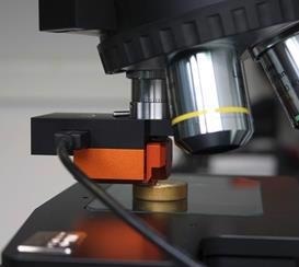
Figure 1. An AFM attachment available from multiple suppliers
Other accessories of Zeta-20 Optical Profilers include:
- Diamond scribe to mark defects
- External dark field illumination
- Edge inspection fixture with dark field illumination
- Through transmissive illumination
- SWIVEL head option
Given below are the major applications of Zeta-20 Optical Profilers:
- Unlike stylus profilers that do not provide information on buried layers, Zeta-20 Optical Profilers can characterize both upper film and the layers beneath (Figure 2).
- Probes may take a longer time to characterize large areas, and their tip shape can vary during scans, leading to inaccurate measurements. Zeta-20 Optical Profilers allow fast large area scans (Figure 3).
- Zeta-20 Optical Profiler exhibits true film colors (Figure 4). Rough surfaces are not a problem and no wear or replacement as there is no stylus
- Unlike a probe, the ZDot™ technology is capable of imaging aromatic oil droplets in Rosemary leaf (Figure 5)
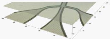
Figure 2. Measurement of layers beneath the material’s surface
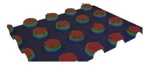
Figure 3. Large area measurement
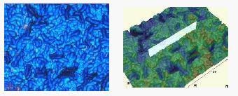
Figure 4. Zeta-20 Optical Profilers exhibit true film colors.
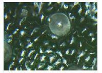
Figure 5. ZDot™ technology can image a Rosemary leaf, showing the aromatic oil droplets.
Conclusion
With ZDot™ optical profiling technology, the concept of confocal microscopy is extended with the additional benefit of true-color imaging. It allows imaging of complex surfaces at ease and provides exceptional metrology capability required for challenging production and R&D applications in the high brightness LEDs, microfluidics, solar cells, advanced semiconductor packaging, and several other sectors.

This information has been sourced, reviewed and adapted from materials provided by KLA Corporation.
For more information on this source, please visit KLA Corporation.