Quality control and testing is a significant and integral part of the manufacturing process of smooth reflective surfaces. The surfaces are studied to look for signs of corrosion, cracks, impurities, dents, and pores. A localized form of corrosion, known as pitting, causes the formation of tiny cavities which can grow deep below the surface.
In this article, the scanning electron microscope VEGA3 integrated with the Alicona MeX 3D Metrology software is used for surface inspection and assessment of pitting in a reflective surface sample of the Atacama Large Millimeter Array (ALMA) telescope.
Procedure
It is possible to obtain a series of images of the sample from different angle viewpoints, by either slightly tilting the electron beam or, alternatively, the sample stage allowing wider angles views. While the former is suitable for short working distances and comparatively flat samples, the latter enables imaging topographic samples and at large working distances. The software subsequently uses the collected images to recover the spatial coordinates of each observed point and, consequently, a true 3D model of the specimen’s surface can be reconstructed. Roughness, profile, volume, area, and Z” height of the sample can be measured using the dataset. These capabilities enable measuring topographical artifacts for surface quality control applications.
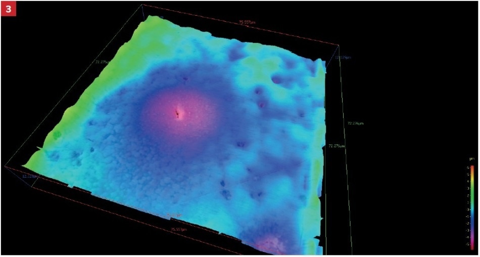
Here, the artifact is a pitting that occurred due to imperfect nickel and gold coating. Surface reconstruction and 3D measurements were carried out to assess the depth of the pitting and to determine whether the damage reaches the main material.
Results
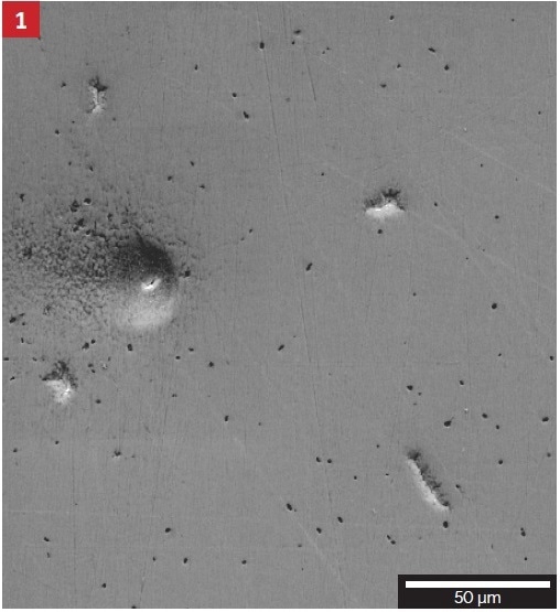
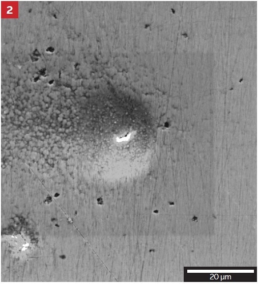
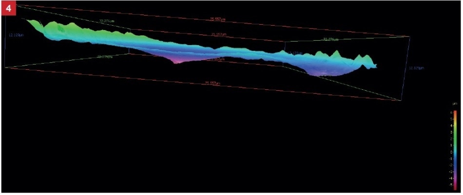
After the profile of the defect shown in Figure 1, 2 was reconstructed (Figures 3, 4), its depth was established to be about 5 μm (Figure 5). This implies that the suitable limit of 0.1 μm for these kind of defects was considerably surpassed.


Further Comments
Further examination of pitting can be complemented using energy dispersive X-ray microanalysis (EDS). The EDS technique can be used to accurately determine the layers which are influenced by pitting. 3D surface reconstruction is not restricted to metal surfaces and can be successfully used in many other applications.


Acknowledgements
Many thanks are due to Frentech Aerospace s.r.o. for offering the sample of a reflective surface.
TESCAN Group
Founded in 1991 by a group of managers and engineers from Tesla with its electron microscopy history starting in the 1950’s, today TESCAN is a globally renowned supplier of Focused Ion Beam workstations, Scanning Electron Microscopes and Optical Microscopes. TESCAN’s innovative solutions and collaborative nature with its customers have won it a leading position in the world of nano- and microtechnology. The company is proud to participate in premier research projects with prominent institutions across a range of scientific fields. TESCAN provides its clients with leading-class products in terms of value, quality and reliability. TESCAN Group is the North American arm of TESCAN Group, a multinational company established by the merger of Czech company TESCAN, a leading global supplier of SEMs and Focused Ion Beam workstations, and the French company ORSAY PHYSICS, a world leader in customized Focused Ion Beam and Electron Beam technology.

This information has been sourced, reviewed and adapted from materials provided by TESCAN Group.
For more information on this source, please visit TESCAN Group.