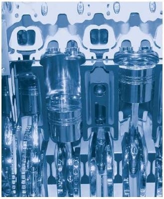
Austempered Ductile Iron (ADI) excels through strength, wear resistance and toughness - characteristics that make ADI the material of choice for use in combustion engines and gear box components. This means that safety aspects are also involved in addition to purely functional aspects. For this reason, changes in the ADI production process need to be monitored with respect to the material's characteristics and must be optimized systematically. For the micro- and nanoscopic analysis of the structure and precipitations, scientists typically use both light and electron microscopes.
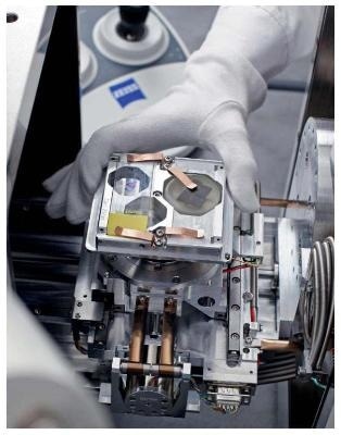
To date, however, there has been no possibility of relocating regions of interest without doubt when transferring the sample from the light to the electron microscope or vice versa. "Shuttle & Find" - the interface for correlative microscopy in materials analysis offers an easy-to-use solution, allowing seamless integration of these two complementary technologies for the first time.
Material - Austempered Ductile Iron
EN-GJS-1200-2 according to DIN EN 1564. Austempered Ductile Iron (ADI) is a family of iron-based materials, which among different processes can be obtained by heat treatment (so-called austempering) of nodular cast iron. ADI is well-known for its excellent strength, wear resistance and toughness. The ultimate tensile strength of min. 1200 MPa and elongation at fracture of min. 2% results in a cost-effective solution providing comparable performance to high strength aluminum alloys (per unit weight) or even steels.
Carl Zeiss Analytical Instruments
The current investigations were done on a ZEISS Axio Imager.M1 light microscope with motorized stage, SUPRA™ 40VP Field Emission-SEM (FE-SEM) equipped with an AsB® detector, SUPRA™ 55VP FE-SEM with an AsB® and Bruker Quantax 200 EDS detectors.
In general, in order to enable the correlative workflow, the following points should be fulfilled:
- Light microscope equipped with digital camera and motorized stage of Axio Imager, Axio Observer and SteREO Discovery families with corresponding mounting frames,
- Scanning electron microscope of EVO®, SIGMA, SUPRA™, ULTRA and MERLIN® families with an SEM adapter for correlative microscopy,
- Correlative holder,
- Software compatibility requirements.
Application
Supporting the tribological characterization the main investigation task was an exact description, including elemental analysis, of the materials microstructure. This was, however, only possible with the help of correlative microscopy, because the (hard) precipitates allowed a systematic investigation in the scanning electron microscope (SEM) after being examined in the light microscope only in case of a precise relocation. In addition, the task became more complicated by the fact that it was only possible to detect the precipitates in the SEM with the backscatter electron detector (e.g. AsB®).
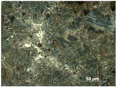
Fig. 1. Light microscope image of ADI sample with a magnification of approx. 400:1. One can see the ROI with the precipitates.
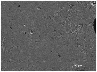
Fig. 2. SE image of the same area as in Fig. 1. The problem of relocating the same area with SE becomes evident.
The identification of the chemical composition of precipitates is possible only by EDS. Thus, the exact relocation of the region of interest (ROI) - in order to avoid time consuming searches - is of great importance. "Shuttle & Find" - correlative microscopy solution from Carl Zeiss fulfills exactly these application requirements and allows micron-precise relocation of the ROI on metallographic samples even at high magnifications in both light and electron microscopes, making subsequent EDS in a SEM a matter of routine (Figs.1-4).
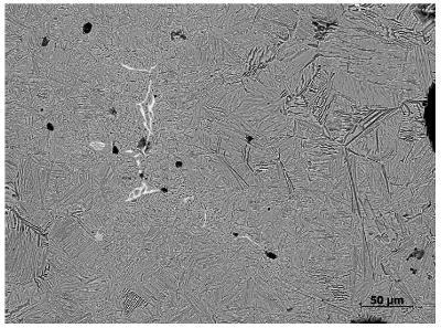
Fig. 3. BSE image of the same area as in Fig. 1.The microstructure is clearly visible in comparison to the SE image.
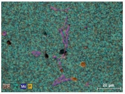
Fig. 4. SE image of the same area as in Fig. 1 overlapped with Mo, Fe and P mappings obtained with EDS.
Results
The matrix basically consists of bainite (in fact ausferrite), graphite nodules and of individual areas of retained austenite. The precipitates were found in these areas. After the relocation of the precipitates in SEM with the help of "Shuttle & Find", the area was scanned with EDS for Mo, Fe, P and C. The spatial resolution of EDS in this experiment is limited in order to provide information about the exact position of the neighboring elements. Nevertheless, the EDS mappings showed that Mo, P and C are found in the same area, verifying the existence of iron phosphides and molybdenum carbides respectively. The wear resistance increases through such hard precipitates whereas the toughness decreases.
Note: The Mo (La) line (2.29 keV) and S (Ka) line (2.31 keV) interfere. An acceleration voltage of 30 kV and a long analysis time are required in order to resolve Mo.
This information has been sourced, reviewed and adapted from materials provided by Carl Zeiss Microscopy GmbH.
For more information on this source, please visit Carl Zeiss Microscopy GmbH.