Mar 21 2019
Topological materials possess extraordinary, defect-resistant properties and are anticipated to be used in quantum computing, optics, electronics, and other domains. Now, the realization of these so-called materials has exposed a new field in materials discovery.
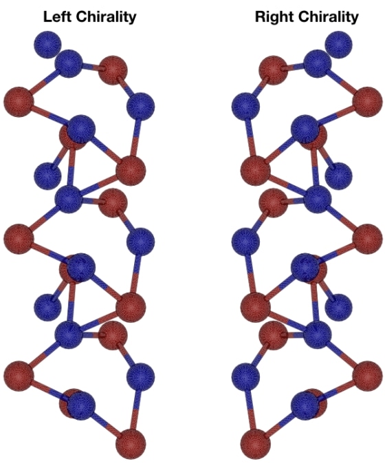
 The spiraling, chiral structure of crystals containing rhodium and silicon. (Image credit: Hasan Lab/Princeton University)
So far, a number of intensely researched topological materials are believed to be topological insulators. It is anticipated that their surfaces will conduct electricity with very minimum resistance, slightly similar to superconductors but without the necessity for extraordinarily chilly temperatures, whereas current is not conducted by their interiors, that is, the so-called “bulk” of the material.
Now, a research team working at the Lawrence Berkeley National Laboratory (Berkeley Lab) of the Department of Energy has identified the most powerful topological conductor to date, in the form of thin crystal samples having a structure of spiral staircase. The researchers’ study of crystals, called topological chiral crystals, has been published in the March 20th, 2019, edition of the journal Nature.
The focus of the new study was the helicoid, or the DNA-like spiraling structure, in the thin crystal sample. This structure displays a chirality or “handedness”—since a person can be either right-handed or left-handed, and the right hand is a mirror image of the left hand. In certain cases, chiral properties can be flipped, similar to a right-handed person becoming a left-handed person.
In this new work we are essentially proving that this is a new state of quantum matter, which is also exhibiting nearly ideal topological surface properties that emerge as a consequence of the chirality of crystal structure.
M. Zahid Hasan, Visiting Faculty Scientist, Materials Sciences Division, Berkeley Lab.
Hasan is a topological materials pioneer who headed the materials theory and experiments. He is also the Higgins Professor of Physics at Princeton University.
A property defining topological conductivity—which is associated with the electrical conductivity of the surface of the material—was determined to be roughly 100 times larger than that seen in the formerly discovered topological metals.
Called the surface Fermi arc, this property was uncovered in X-ray experiments at the Advanced Light Source (ALS) of Berkeley Lab with the help of a method called photoemission spectroscopy. The synchrotron, ALS¸ generates powerful light—right from infrared rays to high-energy X-rays—for many numbers of concurrent experiments.
Topology is known to be a proven mathematical concept relating to the preservation of the geometrical properties of an object even if an object is deformed or stretched in other manners. A few of its experimental uses in 3D electronic materials, like identifying topological behaviors in the electronic structures of materials, were achieved only in the past 10 years, with Berkeley Lab’s early and ongoing contributions.
After more than 12 years of research in topological physics and materials, I do believe that this is only the tip of the iceberg. Based on our measurements, this is the most robust, topologically protected conductor metal that anybody has discovered—it is taking us to a new frontier.
M. Zahid Hasan, Visiting Faculty Scientist, Materials Sciences Division, Berkeley Lab.
The term “topologically protected” implies that certain properties of the material are consistently constant even if the material in question is imperfect. The same quality also strengthens the future potential of manufacturability and practical applications for such kinds of materials.
Princeton researcher Ilya Belopolski, who took part in both the experimental and theoretical work, observed that a specifically fascinating property of the analyzed crystals, containing rhodium-silicon and cobalt-silicon crystals, is that they are capable of creating an electrical current of a fixed strength when a light is illuminated on them.
Our previous theories showed that—based on the material’s electronic properties that we have now observed—the current would be fixed at specific values. It doesn’t matter how big the sample is, or if it’s dirty. It is a universal value. That’s amazing. For applications, the performance will be the same.
Ilya Belopolski, Researcher, Princeton University.
In earlier experiments conducted at the ALS, Hasan’s group demonstrated the existence of a type of massless quasiparticles called Weyl fermions, which so far had been known to exist in theory for approximately 85 years.
Artificial crystals of a semimetal, known as tantalum arsenide, contain the Weyl fermions, which display certain analogous electronic properties to those observed in the crystals applied in the new research, yet lacked their chiral properties. Semimetals are a group of materials that contain some non-metal and metal properties.
“Our earlier work on Weyl semimetals paved the path for research on exotic topological conductors,” stated Hasan.
In a study carried out in November 2017 that was focused on the concept surrounding these unusual materials, Hasan’s group estimated that electrons in rhodium-silicon as well as numerous associated materials behaved in rather unique ways.
It was predicted by the team that quasiparticles in the material—elucidated by the overall movement of electrons—evolved like massless electrons and should act like slowed, three-dimensional (3D) light particles, with definite chirality or handedness properties that are different from graphene or topological insulators.
Moreover, the team’s calculations reported on October 1st, 2018, in the Nature Materials journal, proposed that within the crystals, electrons would collectively act as if they are magnetic monopoles in their movement. Magnetic monopoles are theoretical particles having one magnetic pole, similar to the Earth lacking a South Pole that can shift independent of a North Pole.
Hasan observed that this extraordinary topological behavior points back toward the crystal samples’ chiral nature; this sample produces a “helicoidal” or spiral electronic structure, as noted in the experiments.
A number of several international sources already prepared the analyzed samples, which contain crystals that measure around a couple of millimeters across. The characterization of the crystals was done by Hasan’s team at Princeton’s Laboratory for Topological Quantum Matter and Advanced Spectroscopy applying a low-temperature scanning tunneling microscope, which is capable of scanning samples at the atomic scale. The samples were subsequently sent to Berkeley Lab.
Before the samples were studied at the ALS, they were subjected to a specialized polishing treatment at Berkeley Lab’s nanoscale science research facility—Molecular Foundry. According to Tyler Cochran and Daniel Sanchez, Princeton University researchers who contributed to the research, samples for such kinds of analyses are usually broken, or “cleaved,” so that they are flat at the atomic level.
However, in this situation, the crystal bonds were extremely strong as the crystals possess a cubic shape. Therefore, team members collaborated with the Molecular Foundry staff to discharge high-energy argon atoms at the samples of crystals to flatten and clean them. Following this, the samples were recrystallized and polished all through a heating process.
At the ALS, two different X-ray beamlines—Beamline 10.0.1 and Beamline 4.0.3—were used by the researchers to expose the extraordinary spin and electronic traits of the crystal samples.
Since the electronic behavior in the crystal samples appears to imitate the chirality in the structure of the crystals, a host of other avenues are there to explore, for example, testing whether superconductivity can be transmitted across other types of materials to the topological conductor, added Hasan.
This could lead to a new type of superconductor, or the exploration of a new quantum effect. Is it possible to have a chiral topological superconductor?
M. Zahid Hasan, Visiting Faculty Scientist, Materials Sciences Division, Berkeley Lab.
In addition, while the topological traits seen in cobalt-silicon and rhodium-silicon crystals in the new study are regarded to be perfect, numerous other materials that have been identified can possibly be examined to estimate their potential for better performance for practical applications, stated Hasan.
“It turns out the same physics might also be possible to realize in other compounds in the future that are more suitable for devices,” he stated.
“It is an immense satisfaction when you predict something exotic and it also appears in the laboratory experiments,” added Hasan, noting his group’s previous successes in estimating the materials’ topological properties. “With definitive theoretical predictions, we have combined theory and experiments to advance the knowledge frontier.”
The Molecular Foundry and Advanced Light Source are DOE Office of Science User Facilities.
The study also included researchers from Louisiana State University; Rigetti Quantum Computing; Peking University, the Collaborative Innovation Center of Quantum Matter, and the University of Chinese Academy of Science in China; Academia Sinica and National Cheng Kung University in Taiwan; and the Max Planck Institute for Chemical Physics of Solids in Germany.
The study was supported by the U.S. Department of Energy’s Office of Science, the National Natural Science Foundation of China, the National Key R&D Program of China, the Key Research Program of the Chinese Academy of Science, Academia Sinica’s Innovative Materials and Analysis Technology Exploration program, the Ministry of Science and Technology in Taiwan’s Young scholar Fellowship Program, National Cheng Kung University in Taiwan, the National Center for Theoretical Sciences in Taiwan, the ERC Advanced Grant, and the UC Berkeley Miller Institute of Basic Research in Science’s Visiting Miller Professorship.

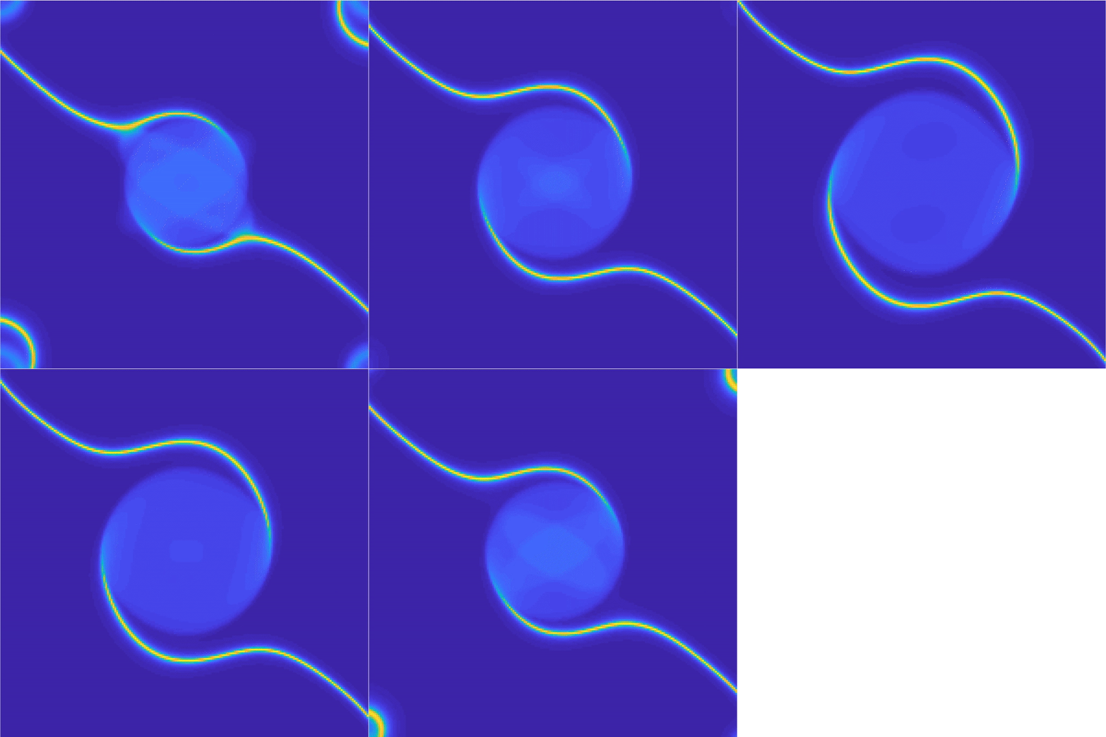
This animation shows how Fermi arc states form a spiraling structure in a crystal material that serves as a topological conductor. (Credit: Hasan Lab/Princeton University)