Apr 29 2019
Scientists at the University of Hamburg and DESY collaborated to perform a research work to develop an appropriate process for 3D printing. It could possibly be used for the production of transparent, mechanically flexible electronic circuits.
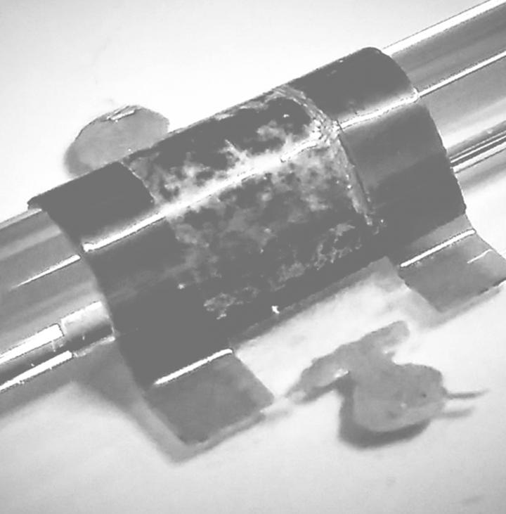
 Example of a flexible and transparent electronic component: a flexible capacitor. (Image credit: University of Hamburg, Tomke Glier)
The electronic circuit is made up of a mesh of silver nanowires that can be used for suspension printing and embedded in many flexible and transparent plastics (polymers). This method can facilitate new applications like solar cells, printable light-emitting diodes, or tools with integrated circuits, as Tomke Glier from the University of Hamburg and her research team reported in Scientific Reports. The scientists have shown the potential of their process with a flexible capacitor, among others.
The aim of this study was to functionalize 3D-printable polymers for different applications. With our novel approach, we want to integrate electronics into existing structural units and improve components in terms of space and weight.
Michael Rübhausen, Center for Free-Electron Laser Science (CFEL)
CFEL is a joint enterprise of DESY, the University of Hamburg, and the Max Planck Society (MPG).
This work was guided by Rübhausen, a physics professor from the University of Hamburg, in collaboration with Stephan Roth from DESY, who is also a professor at the Royal Institute of Technology in Stockholm. The researchers, with the help of the bright X-ray light from DESY’s research light source PETRA III and other measuring methods, have exactly analyzed the properties of the nanowires in the polymer.
“At the heart of the technology are silver nanowires, which form a conductive mesh,” stated Glier. The thickness of silver wires is usually several tens of nanometers (one-millionth of a 1 mm) and their length is 10–20 µm (one-thousandth of 1 mm). The thorough X-ray analysis reveals that their structure in the polymer is unchanged; however, the conductivity of the mesh also improves due to the compression by the polymer, because of the shrinkage of the polymer during the curing process.
The silver nanowires carried in suspension are applied to a substrate and dried. Roth, head of the P03 measuring station at DESY’s X-ray light source PETRA III, where the investigations of the X-ray were carried out, explained, “For cost reasons, the aim is to achieve the highest possible conductivity with as few nanowires as possible. This also increases the transparency of the material. In this way, layer by layer, a conductive path or surface can be produced.”
A flexible polymer is applied to the conductive tracks and then is possibly covered with contacts and conductive tracks. On the basis of the geometry and material used, several electronic components can be printed in this manner.
In this study, the scientists designed a flexible capacitor.
In the laboratory, we carried out the individual work steps in a layering process, but in practice they can later be completely transferred to a 3D printer.
Tomke Glier, University of Hamburg
“However, the further development of conventional 3D printing technology, which is usually optimized for individual printing inks, is also essential for this. In inkjet-based processes, the print nozzles could be clogged by the nanostructures,” observed Rübhausen.
Moving forward, the scientists intend to test how the structure of the conductive paths comprising of nanowires changes under mechanical stress. “How well does the wire mesh hold together during bending? How stable does the polymer remain,” stated Roth, referring to standard questions. “X-ray investigation is very suitable for this because it is the only way we can look into the material and analyze the conductive paths and surfaces of the nanowires.”
This study was carried out by the scientists from the University of Hamburg, the Royal Institute of Technology in Stockholm, the Wallenberg Centre for Wood Science in Stockholm, the Max Planck Institute for the Structure and Dynamics of Matter in Hamburg, and DESY.