Due to their ultra-thin thickness, dangling-bond-free flat surface, and superior gate controllability, two-dimensional (2D) semiconductors, such as MoS2, open up previously unimaginable possibilities for overcoming the transistor scaling bottleneck and creating novel logic circuits with increased speed, reduced power consumption, flexibility, and transparency.
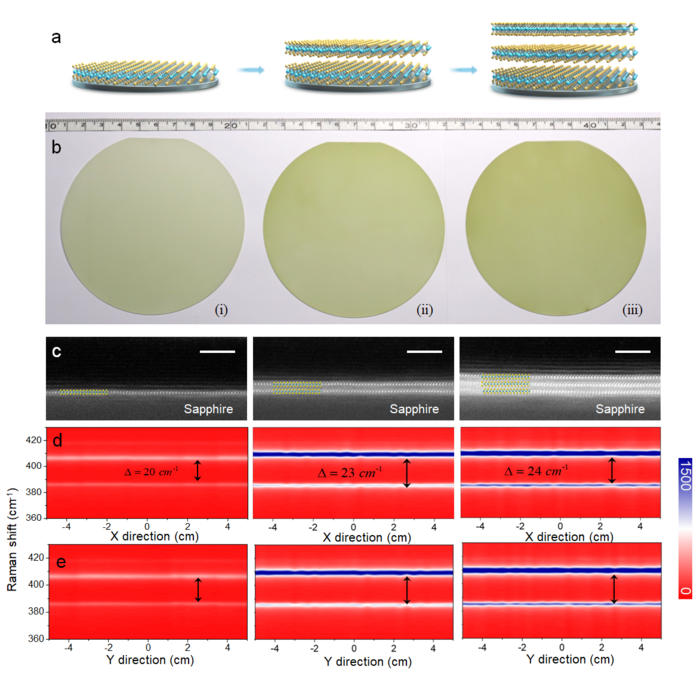
 (a) Schematic illustration of epitaxy process. (b) Photographs of 4-inch MoS2 wafers: monolayer (i), bilayer (ii), trilayer (iii). (c) Cross-sectional HAADF-STEM images of epitaxial mono-, bi- and trilayer MoS2. Scale bars: 3 nm. (d, e) Color-coded images of typical Raman line scan mapping along the horizontal (d) and longitudinal direction (e) of monolayer (left panel), bilayer (middle panel) and trilayer MoS2 (right panel). Image Credit: Science China Press
The International Technology Roadmap for Semiconductors (ITRS) report in 2015 made it abundantly evident that 2D semiconductors are essential components of the upcoming high-performance devices. In 2021, Intel identified 2D MoS2-based transistor technology as one of the three game-changing innovations for the next ten years.
Massive efforts have been made to investigate the calibrated potentials of monolayer MoS2, such as the large-area devices and the wafer-scale fabrication of high-quality materials. The structural flaws in the large-scale monolayer MoS2 should be reduced as much as possible to enhance its electrical quality; however, after 10 years of synthesis optimizations in this area, there is not much room left for monolayer MoS2.
Switching to multilayer MoS2, such as bilayers and trilayers, is another important step since they naturally have greater electrical quality than monolayers and are therefore more suitable for higher-performance devices and logic circuits.
However, it is still very difficult to create wafer-scale multilayer MoS2 with excellent quality and widespread uniformity because of the underlying thermodynamics constraint.
According to a study that was published in National Science Review, a research team from China has resolved the basic restrictions of thermodynamics by taking advantage of the proximity effect of the substrate and has successfully grown high-quality multilayer MoS2 4-inch wafers using the layer-by-layer epitaxy process for the first time.
The epitaxy results in clearly defined stacking orders between neighboring epitaxial layers and provides exquisite control of layer numbers up to six.
To achieve the layer-by-layer epitaxy of multilayer MoS2, we independently design an oxygen-assisted 4-inch multi-source CVD system. The breakthrough of controllable epitaxy of high-quality multilayer MoS2 wafers would lay a solid material foundation for large-scale high-performance 2D electronic devices, and is expected to play a paramount role in sub-10 nm ultra-short channel devices, flexible displays and smart wearable devices.
Dr. Qinqin Wang, Study First Author, Beijing National Laboratory for Condensed Matter Physics and Institute of Physics, Chinese Academy of Sciences
MoS2 field-effect transistors with thicker layers display considerable gains in device performance over monolayers. The average field-effect mobility for long-channel devices can rise from ~80 cm2 V–1 s–1 for monolayers to ~110/145 cm2 V–1 s–1 for bilayer/trilayer devices, an improvement of 37.5 V /81.3 V.
The maximum room temperature mobility for trilayer MoS2 field-effect transistors may reach up to 234.7 cm2V–1s–1, breaking the previous record for 2D TMS semiconductor devices.
Current density (Vds=1 V) for devices with a channel length of 100 nm is raised from 0.4 mA μm–1 for monolayer to 0.64/0.81 mA μm–1 for bilayer/trilayer, exhibiting an enhancement factor of 60%/102.5%.
Notably, trilayer MoS2 field-effect transistors are capable of achieving record-high on-current densities of 1.70/1.22/0.94 mA/μm at Vds=2/1/0.65 V as well as a high on/off ratio surpassing 107.
Considering that, in well-developed thin-film transistors (TFTs), field-effect mobility is 10–40 cm2·V–1·s–1 for indium–gallium–zinc-oxide TFTs and 50–100 cm2·V–1·s–1 for low-temperature polycrystalline silicon TFTs, the competitive average field-effect mobility, e.g., larger than 100 cm2·V–1·s–1, achieved in this work strongly uncover a great potential of these multilayer MoS2 films for high-performance TFT applications.
Dr. Jian Tang, Study Lead Author, Beijing National Laboratory for Condensed Matter Physics and Institute of Physics, Chinese Academy of Sciences
The on-current density of trilayer MoS2 devices with a channel length of 40 nm can reach a record-high value of 1.70 mA/μm at Vds=2 V, outperforming the previous state-of-the-art MoS2 transistors. Such high on-current density also exceeds the target of high-performance logic transistors from the International Roadmap for Devices and Systems (IRDS) 2028, and hence moves a step closer to practical applications of 2D MoS2 in electronics and logic circuits at sub-5 nm nodes.
Guangyu Zhang, Professor, Institute of Physics, Chinese Academy of Sciences
Journal Reference:
Wang, Q., et al. (2022) Layer-by-layer epitaxy of multi-layer MoS2 wafers. National Science Review. doi:10.1093/nsr/nwac077.