In the fields of electronics and nanotechnology the ability to manipulate materials at the nanoscale is paramount. Focused ion beam (FIB) instruments have become essential for this work.
FIB works in a similar way to scanning electron microscopy (SEM), but instead of scanning electrons over a surface, an ion beam is used. As the focussed ion beam is more energetic than an electron beam it can directly alter or ‘mill’ the surface of a sample via a sputtering process, which can be precisely controlled at a nanometre accuracy. This allows the ion beam to be used for detailed nano-machining, to remove material (milling) or to produce minute components or shapes (fabricating).
Material can be added to a surface at high precision using a FIB, via a process named ion beam assisted chemical vapor deposition (CVD). This is, in effect, the reverse of FIB milling. Ion beam assisted CVD uses a specific deposition gas, which decomposes to deposit material on the sample surface in a precise fashion.
A Dual System that Combines FIB with SEM
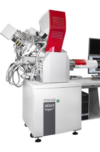
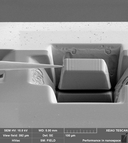
FIB is rarely used alone, and is often combined with an imaging system such as SEM to validate the structures fabricated by the FIB. The XEIA3 from Tescan includes an SEM column for real-time imaging during or following ion beam modification; and a micro-manipulator to remove small particles for further analysis.

The XEIA3 from TESCAN
FIB-SEM facilitates the high-resolution SEM imaging of specific areas of an FIB-milled surface by providing complementary imaging and beam chemistry capabilities. This allows selective site sample preparation along with simultaneous SEM imaging and the fabrication of intricate features using sputtering and deposition.
Why FIB using Xenon is Advantageous
Conventional FIB systems use a finely focused beam of gallium ions for sample surface milling. However, FIB using a xenon ion plasma, in the place of gallium, has been shown to be preferable for many applications.
Gallium beams inherently implant gallium atoms into the surface layers of the sample being milled. This is problematic as it can contaminate the sample's crystal structure, change its shape (amorphisation) and, because gallium is conductive, it can also result in changes in the sample's electrical behaviour.
This is not an issue with Xe plasma FIB as xenon implants less due to its chemical inertness, and xenon’s low conductivity means the samples electrical behaviour remains unchanged. This means that Xe plasma FIB, even at 30 keV energy and 60 nA current, does not result in significant sample amorphisation or phase changes. The xenon beam can also achieve a much faster milling rate, which can be 60 times faster than gallium, which means large sections of samples and deeper sample depths can be reached.
TEM Sample Preparation with Xe Plasma FIB
Transmission electron microscopy (TEM) is a nanoscale imaging technique that involves the transmission of electrons through a sample, which are then measured to create an image. To ensure enough electrons are transmitted to create a useful image the sample used must be extremely thin, often thinner than 100 nm.
TEM can be used to capture fine details in a sample and, as electrons passing through the sample are diffracted, it can also be used to observe crystal dislocations and other structural irregularities in the sample. As a result, TEM is routinely used in materials science, especially in the fields of nanotechnology and semiconductor research.
One of the major applications of FIB is the preparation of samples for TEM imaging. For this application, FIB induced damage on the sample must be avoided as this would create an unrepresentative sample structure. This is especially true for detailed and complex systems such as those seen in the microelectronics industry. In these instances, the use of a low energy Xe beam is preferable.
Research has demonstrated that using a Xe beam for the preparation of lamellae samples produces significantly less damage at a 30 keV beam energy than a Ga beam. In addition to this the Xe beam provided higher quality lamellae samples and required significantly less finishing.
Fabrication of a Micro-Hall Probe using Xe Plasma FIB
Hall probes are transducers which are able to vary their output voltage in response to the proximity of a magnetic field via a mechanism known as the Hall Effect. As Hall probes produce electronic responses to magnetism they are an ideal sensing technology for the detection of magnetic fields.
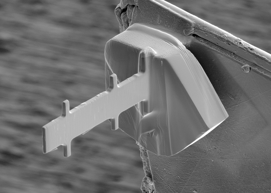
Hall probes are produced using a thin sheet of semi-conductive material such as tantalum phosphide (TaP). Producing a micro-scale Hall probe involves a number of challenges such as the risk of changing the materials conductivity, as well as the requirement of a precise technique to mill the material. The TESCAN UHR-SEM/plasma FIB XEIA3 microscope can be used to prepare a micro-scale Hall probe from an ingot of TaP.
In this instance the use Xe plasma FIB was particularly useful as the use of a Xe beam allowed for milling at a higher current of 2 μA, which is significantly higher than the maximum current allowed by a Ga FIB of 50 nA. This means that a 100 μm3 volume of silicon can be sputtered by Xe-FIB in only 18 minutes, whereas with Ga-FIB this would take 19 hours.
Additionally, if xenon is implanted into the material during the sputtering process the result is inconsequential. As xenon does not conduct there will be no changes to the potential and current measurements of the Hall probe. Whereas if gallium were to contaminate the sample this could result in erroneous probe measurements.

A micro-hall probe fabricated using the TESCAN XEIA3
Conclusion
The applications for the combination FIB-SEM instruments are varied, ranging from particle analysis and material characterisations, to industrial failure analysis and process control. Xe FIB shows many major benefits over Ga FIB due to its low contamination, speed and high controllability.
The Tescan XEIA3 combines high resolution imaging with rapid and controllable micromachining.
Download the Brochure for More Information
References & Further Reading
- C.A. Volkert and A.M. Minor, Focused Ion Beam: Microscopy and Micromachining, MRS Bulletin, 2007, 32: 389–399.
- T.L.Burnett, R.Kelley, et al., Large volume serial section tomography by Xe Plasma FIB dual beam microscopy, Ultramicroscopy, Volume 161, February 2016, Pages 119-129
- Tomáš Hrnčíř, Jozef Vincenc Oboňa, et al., How Xe and Ga FIB Differ in Inducing Lateral Damage on TEM Samples, ISTFA 2015: Proceedings from the 41st International Symposium for Testing and Failure Analysis (November 1–5, 2015, Portland, Oregon, USA)
- B. D.A. Levin; et al. (2016). "Nanomaterial datasets to advance tomography in scanning transmission electron microscopy". Scientific Data. 3: 160041.
- Tescan application note, Hall probe preparation from TaP using Xe Plasma FIB, 2018
TESCAN Group
Founded in 1991 by a group of managers and engineers from Tesla with its electron microscopy history starting in the 1950’s, today TESCAN is a globally renowned supplier of Focused Ion Beam workstations, Scanning Electron Microscopes and Optical Microscopes. TESCAN’s innovative solutions and collaborative nature with its customers have won it a leading position in the world of nano- and microtechnology. The company is proud to participate in premier research projects with prominent institutions across a range of scientific fields. TESCAN provides its clients with leading-class products in terms of value, quality and reliability. TESCAN Group is the North American arm of TESCAN Group, a multinational company established by the merger of Czech company TESCAN, a leading global supplier of SEMs and Focused Ion Beam workstations, and the French company ORSAY PHYSICS, a world leader in customized Focused Ion Beam and Electron Beam technology.

This information has been sourced, reviewed and adapted from materials provided by TESCAN Group.
For more information on this source, please visit TESCAN Group.