Material fabrication processes can gradually create changes in the material’s final properties; thus, to verify the material’s final quality and comprehend any inconsistencies, scientists need a statistically relevant sample count to attain sufficient analytical data. For the accurate assessment of total material quality, several samples from different regions of the material may need to be investigated.

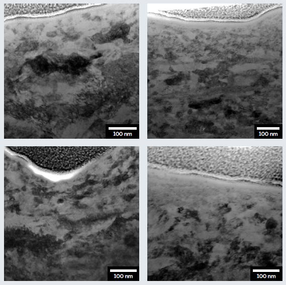
Figure 1. STEM Angular Dark Field images of titanium TEM samples prepared automatically with TESCAN AutoSlicer™ software to the average thickness of 65 nm. Image Credit: TESCAN Group.
The total volume required for comprehensive characterization depends on the size of the features needed to be investigated. These feature sizes are often nanometer scale, meaning changes in phase and chemical composition, or changes in the material’s morphology, require high-resolution instrumentation for proper study.
The development of new materials means new sample characterization challenges. An ultra-high-resolution technique is required to study materials with grain sizes in the tens of nanometers.
Electron microscopy is often the initial choice when nanometer-scale resolution is required for capturing finer details crucial for understanding a material’s properties. Transmission electron microscopy (TEM) offers the ultimate resolution and is quickly becoming the technique of choice for highly detailed materials characterization. For TEM characterization, the sample must be transparent to incident electrons. Attaining the correct sample thickness uniformity with limited amorphous damage is crucial for achieving optimal analytical results.
Employing FIB-SEM to prepare samples means precise navigation to areas of interest. Since it is a site-specific technique, FIB-SEM will not cause damage outside of the targeted areas. Multiple TEM samples can therefore be prepared from nearby locations on the sample. With this approach, the physical mechanical properties of materials can be assessed with more accuracy because there are enough samples.
TEM sample preparation by FIB-SEM may be challenging for users with less experience, and TEM sample quality may be questioned. To avoid this, Tescan uses an automated process for TEM sample preparation. This ensures reproducible TEM sample quality, saves the operator time, and allows those lacking extensive FIB-SEM experience to prepare high-quality TEM samples.
Materials and Methods
Titanium material with a very fine grain structure was utilized for analysis. Numerous titanium samples were prepared for TEM characterization. The titanium sample has a very fine grain structure, meaning TEM analysis is likely to reveal further detail regarding the sample surface compared to the commonly employed EBSD characterization.
Four TEM lamellae were prepared from different parts of the titanium sample utilizing automated processes specified in a single job template. TEM samples were prepared by two FIB-SEM operators utilizing the Ga-ion TESCAN AMBER FIB-SEM with integrated TESCAN AutoSlicer™ software for TEM sample preparation.
TESCAN’s AutoSlicer™ automates in-trench preparation and final polishing to guarantee that samples are prepared with reliable quality. TEM sample lift-out and attachment to the TEM grid are conducted using a guided, step-by-step workflow found in the software to preserve a reliable workflow and minimize the potential for operator error.
TESCAN TENSOR STEM was utilized for TEM characterization and to ascertain the average grain size of analyzed materials, creating statistical information about the material’s grain size. Information about the average grain size is key when modeling the materials’ properties under different conditions, such as chemical and mechanical changes at specific temperatures, or mechanical loads.
Another important parameter that can be evaluated is maximum grain size, which may substantially alter materials’ properties locally when it varies greatly from the average grain size.
The 4D-STEM technique allows the study of materials’ crystallography at the nanoscale. The fully integrated 4D detector reveals grain orientation, size, and phase. This method was used for the crystallographic study of the titanium samples.
Results and Discussion
The four TEM samples were thinned to transparency using TESCAN AutoSlicer™. TEM samples were prepared automatically in-trench, including the automated undercut and the initial polishing step. After the undercut, the step-by-step workflow guides the operator through the lift-out and attachment to the TEM grid, reducing the risk of losing the prepared TEM sample. Once the sample is attached to the grid, the final polishing steps can begin.
TEM samples are usually polished at high keV to reduce TEM sample thickness, followed by low keV polishing to reduce amorphization. In this study, automated high keV polishing was followed by automated low keV cleaning to prepare the titanium samples. No further polishing step was necessary to improve TEM sample quality.
The conditions and steps used are chosen by the operator and can be altered as needed for the material being investigated. Reproducible final quality for all four samples was proven through the measurement of cross-section thickness in the FIB-SEM, and TEM analyses. The average thickness of these TEM samples prepared using the automated procedure and guided lift-out was 65 nm ±9 nm.

Figure 2. STEM Bright Field detail images showing the very fine grain structure of the titanium material. Image Credit: TESCAN Group.

Figure 3. Corresponding grain orientation maps from the detail images shown in Figure 2. Image Credit: TESCAN Group.
Conclusions and Outlook
The final quality of the prepared samples is the main concern for any sample that will be analyzed using TEM. Automation of the sample preparation process ensures that the sample quality is reproducible and greatly increases throughput when many samples are required. Processing with automation also decreases the potential for errors during sample preparation that could influence incorrect assumptions about material properties.
The automation also enables users with less FIB-SEM experience to confidently prepare samples. TESCAN AutoSlicer™ was designed for the easy customization of recipes, and the sharing of presets and complete workflows with other users.

This information has been sourced, reviewed and adapted from materials provided by TESCAN Group.
For more information on this source, please visit TESCAN Group.