Jul 16 2008
Ferroelectric materials are named after ferromagnetic ones because they behave in a similar way. The main difference: these materials are not magnetic, but permanently electrically polarized. They have great importance for data storage technology and novel piezoelectric devices. Dresden scientists were able to produce microscopic images of ferroelectric domains - tiny regions of a ferroelectric material -, where the electric polarization points into different directions. These results were published in the journal “Physical Review Letters” recently.
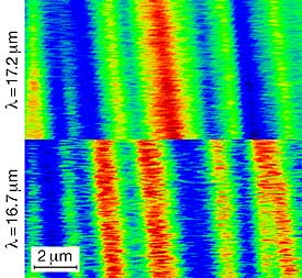
 False color image of the electric domains on the surface of a bariumtitanate crystal.
Dr. Lukas M. Eng and his group at the Technische Universität Dresden used the free-electron laser at the Forschungszentrum Dresden-Rossendorf (FZD) to study ferroelectric domains. Ferroelectric materials are special crystals like, e.g. bariumtitanate, where the titanium atoms in the crystal lattice are slightly shifted into one direction. This shift results in a polarization and, therefore, in a permanent electric field. The ferroelectric domains differ only by the direction of the permanent electric field in the material. The two possible types of domains show either an electric field which is oriented parallel to the surface of the crystal or which points perpendicular to the surface. By applying an external field (e.g. electric voltage) one can reverse the polarity of the domains. Because of these properties ferroelectric materials are widely used in novel technological devices, such as in Ferroelectric Random Access Memory (FRAM or FeRam).
The Dresden scientists aimed at getting as clear an image as possible of the domains in order to understand better how they function, and to specifically manipulate the electric charge of the domains for future devices. The size of a bariumtitanate domain is about one to ten micrometers. Optical methods are dependent on the wavelength of the type of “light” which is applied. The free-electron laser at the FZD emits powerful radiation in a wide range of the infrared and THz region of the electromagnetic spectrum – a region where not many other laser sources exist. The scientists tuned the laser to a frequency which was in resonance with the atomic motion in the bariumtitanate (near 18 Terahertz). Then they shone the invisible laser beam onto a sharp needle (the tip of an atomic force microscope), moving across the sample surface. Finally they measured the light that was scattered away from the needle. It turns out that this signal contains microscopic information about the sample, in fact with a resolution better than 200 nanometers, which is hundred times smaller than the wavelength of the light.
The domains of the ferroelectric material shimmered in different colors. This is due to the fact that the interaction of the infrared light with the crystal via the tip is different for the two types of domains. The technique itself is called near-field microscopy. The researches were taking advantage of the fact that the two types of domains have their individual resonance frequency. This is the frequency at which the largest amount of infrared light is scattered. In the experiment, areas that appear bright in the image (red in false-color) at a wavelength of 16.7 micrometers, become dark (blue in false color), if the wavelength is tuned to 17.2 micrometers, and vice versa.
The results show the huge potential the free-electron laser has when used for near-field microscopy. The large power and tunability are indispensable for this type of investigations. The group is presently extending its activities thanks to funding by the German Science Foundation (DFG). The scientists of TU Dresden and FZD envision applications for other novel material systems like the so-called multi-ferroics, but also for biomolecules or semiconductor nanostructures (e.g. for wafer inspection).