Sep 15 2009
Today KLA-Tencor Corporation (NASDAQ:KLAC), the world's leading supplier of process control and yield management solutions for the semiconductor and related industries, introduced the Teron 600 Series reticle (mask) defect inspection systems. Addressing a major transition in mask design at the 2Xnm logic (3Xnm half-pitch memory) node, the new Teron 600 platform will introduce programmable scanner-illumination capability and offer significant improvements in sensitivity and computational lithography power over the current industry-standard platform, TeraScanTMXR. These advances are necessary to enable development and manufacturing of the innovative reticles that distinguish the 2Xnm node.
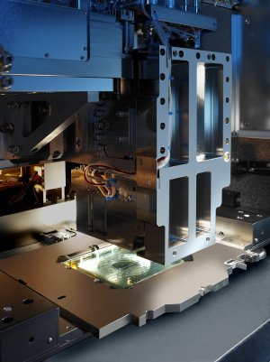
 KLA-Tencor's new Teron 600 reticle defect inspection platform features innovations in imaging and computational lithography, enabling mask manufacturers to develop and produce reticles to support the wide variety of proposed 2Xnm lithography technologies. (Photo: Business Wire)
Traditionally mask designers have started with a mask pattern that looks like the target wafer pattern, making small adjustments to the mask features (optical proximity corrections or OPC) until the desired wafer structures are achieved. This approach begins to break down at the 2Xnm node, as a consequence of extending 193nm lithography into an extreme sub-wavelength regime. Thus, at the 2Xnm node, computational lithography techniques such as Inverse Lithography Technology (ILT) and Source Mask Optimization (SMO) become viable. ILT typically generates a complex mask pattern with an enormous number of very small features, making the mask difficult to manufacture. To complicate matters even further, Source Mask Optimization (SMO) involves calculating a non-uniform intensity profile for the scanner source. That profile is designed to work together with the ILT mask to deliver the optimum lithographic results on the wafer.
“The dramatic change in reticle strategy for the 2Xnm device generation has created a discontinuity in reticle defect inspection,” remarked Brian Haas, vice president and general manager of the Reticle and Photomask Inspection Division at KLA-Tencor. “The reticle features are much smaller than you would predict from a 3Xnm to 2Xnm shrink. In addition, the mask pattern is so fractured that it is no longer feasible for an engineer to look at the location of a reticle defect and decide whether it is likely to print on the wafer—and potentially cause a catastrophic yield loss in the fab. For the 2Xnm node, we must be able to input a custom scanner illumination profile, take into account polarization effects and the photoresist, and rigorously calculate the impact of the reticle defect on the wafer. The Teron 600 leverages KLA-Tencor's strength in computational lithography and our experience from developing and manufacturing six generations of reticle inspection platforms. As a result it is an extremely high-resolution, low-noise reticle inspection system, equipped for the new 2Xnm challenges. It's a big achievement for KLA-Tencor which we believe will be tremendously enabling for our customers and the industry.”
The Teron 600 platform has also been designed for flexibility and extendibility. The system has successfully inspected prototype reticles created for ILT / SMO, double-patterning lithography (DPL), and EUV (masks and blanks). The system is engineered to be extendible to potential 1Xnm optical solutions. Moreover, the Teron 600 Series can work with KLA-Tencor's TeraScan 500 Series reticle defect inspection systems in a mix-and-match strategy, to provide a cost-effective solution for manufacturing photomask sets that include both critical and non-critical layers.
The new Teron 600 Series reticle defect inspection systems will include several features designed to enable production of advanced optical masks and development of EUV masks, including:
- New 193nm wavelength, smaller pixel, improved image processing and ultra-low noise operation to provide high-resolution reticle plane inspection (RPI);
- Die-to-database and die-to-die operating modes, enabling defect capture throughout the die and on a broad range of reticle layouts;
- Wafer-plane inspection (WPI) for prediction of reticle defect printability, complete with photoresist thresholding and modeling of sub-wavelength diffraction and polarization effects;
- New user-configurable scanner illumination model, enabling prediction of reticle defect printability when SMO, ILT or other non-standard scanner illumination geometry is implemented;
- Aerial-plane filtering of nuisance defects, facilitating early process development and faster cycle time during mask production; and
- Compatibility between Teron and TeraScan platforms, for capacity optimization and effective integration of data from critical and non-critical layers.
For more information on how the Teron 600 Series reticle defect inspection systems enable photomask manufacturers to produce and ship masks free from printable defects at the 2Xnm node, please visit the product web page at: http://www.kla-tencor.com/reticle/teron-600.html.