Oct 22 2009
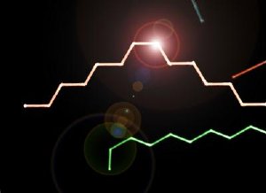
Taking nanomaterials to a new level of structural complexity, scientists have determined how to introduce kinks into arrow-straight nanowires, transforming them into zigzagging two- and three-dimensional structures with correspondingly advanced functions.

The work is described this week in the journal Nature Nanotechnology by Harvard University researchers led by Bozhi Tian and Charles M. Lieber.
Among other possible applications, the authors say, the new technology could foster a new nanoscale approach to detecting electrical currents in cells and tissues.
"We are very excited about the prospects this research opens up for nanotechnology," says Lieber, Mark Hyman, Jr. Professor of Chemistry in Harvard's Faculty of Arts and Sciences. "For example, our nanostructures make possible integration of active devices in nanoelectronic and photonic circuits, as well as totally new approaches for extra- and intracellular biological sensors. This latter area is one where we already have exciting new results, and one we believe can change the way much electrical recording in biology and medicine is carried out."
Lieber and Tian's approach involves the controlled introduction of triangular "stereocenters" -- essentially, fixed 120º joints -- into nanowires, structures that have previously been rigidly linear. These stereocenters, analogous to the chemical hubs found in many complex organic molecules, introduce kinks into 1-D nanostructures, transforming them into more complex forms.
The researchers were able to introduce stereocenters as nanowires self-assembled. They halted growth of the 1-D nanostructures for 15 seconds by removing key gaseous reactants from the chemical brew in which the process was taking place, replacing these reactants after joints had been introduced into the nanostructures. This approach resulted in a 40 percent yield of bent nanowires, which can then be purified to achieve higher yields.
"The stereocenters appear as 'kinks,' and the distance between kinks is completely controlled," says Tian, a research assistant in Harvard's Department of Chemistry and Chemical Biology. "Moreover, we demonstrated the generality of our approach through synthesis of 2-D silicon, germanium, and cadmium sulfide nanowire structures."
The research by Lieber and Tian is the latest in a years-long effort by scientists to control the composition and structure of nanowires during synthesis. Despite advances in these areas, the ability to control the design and growth of self-assembling nanostructures has been limited.
Lieber and Tian's work takes the formation of 2-D nanostructures a step further by enabling the introduction of electronic devices at the stereocenters.
"An important concept that emerged from these studies is that of introducing functionality at defined nanoscale points for the first time -- in other words, nanodevices that can 'self-label,'" Lieber says. "We illustrated this novel capability by the insertion of p-n diodes and field-effect transistors precisely at the stereocenters."
Such self-labeled structures could open up the possibility of introducing nanoelectronics, photodetectors, or biological sensors into complex nanoscale structures.
Lieber and Tian's co-authors are Ping Xie and Thomas J. Kempa of Harvard's Department of Chemistry and Chemical Biology and David C. Bell of Harvard's Center for Nanoscale Systems. Their work was funded by the National Institutes of Health, the McKnight Foundation, the MITRE Corporation, and the National Science Foundation.