Jul 22 2010
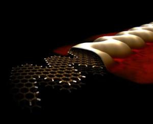
In the recent issue of Nature, scientists from Empa and the Max Planck Institute for Polymer Research report how they have managed for the first time to grow graphene ribbons that are just a few nanometres wide using a simple surface-based chemical method.
Graphene ribbons are considered to be «hot candidates» for future electronics applications as their properties can be adjusted through width and edge shape.

Transistors on the basis of graphene are considered to be potential successors for the silicon components currently in use. Graphene consists of two-dimensional carbon layers and possesses a number of outstanding properties: it is not only harder than diamond, extremely tear-resistant and impermeable to gases, but it is also an excellent electrical and thermal conductor. However, as graphene is a semi-metal it lacks, in contrast to silicon, an electronic band gap and therefore has no switching capability which is essential for electronics applications. Scientists from Empa, the Max Planck Institute for Polymer Research in Mainz (Germany), ETH Zürich and the Universities of Zürich und Bern have now developed a new method for creating graphene ribbons with band gaps.
Extremely narrow graphene ribbons
To date, graphene ribbons have been «cut» from larger graphene sheets, akin to tagliatelle being cut from pasta dough. Or carbon nanotubes were slit open lengthwise and unfurled. This gives rise to a band gap via a quantum mechanical effect - the gap being an energy range that cannot be occupied by electrons and which determines the physical properties, such as the switching capability. The width (and edge shape) of the graphene ribbon determines the size of the band gap and thereby influences the properties of components constructed from the ribbon.
If extremely narrow graphene ribbons (well under 10 nanometres wide) that also have well-defined edges could be manufactured, so the reasoning, then they might allow for components exhibiting specific optical and electronic properties: depending on requirements, adjustment of the band gap could be used to fine-tune the switching characteristics of a transistor. This is no mean feat, as the lithographic methods that have been used until now, for example for cutting graphene layers, come up against fundamental barriers; they yield ribbons that are too wide and have diffuse edges.
Growing graphene ribbons
In the issue of Nature published on 22 July 2010, scientists led by Roman Fasel, Senior Scientist at Empa and Professor for Chemistry and Biochemistry at the University of Bern, and Klaus Müllen, Director at the Max Planck Institute for Polymer Research, describe a simple surface-based chemical method for creating such narrow ribbons without the need for cutting, in a bottom-up approach, i.e. from the basic building blocks. To achieve this, they spread specifically designed halogen-substituted monomers on gold and silver surfaces under ultrahigh vacuum conditions. These are linked to form polyphenylene chains in a first reaction step.
In a second reaction step, initiated by slightly higher heating, hydrogen atoms are removed and the chains interconnected to form a planar, aromatic graphene system. This results in graphene ribbons of the thickness of a single atom that are one nanometre wide and up to 50 nm in length. The graphene ribbons are thus so narrow that they exhibit an electronic band gap and therefore, as is the case with silicon, possess switching properties - a first and important step for the shift from silicon microelectronics to graphene nanoelectronics. And if this wasn't enough, graphene ribbons with different spatial structures (either straight lines or with zig-zag shapes) are created, depending on which molecular monomers the scientists used.
Further studies will help identify properties
As the scientists can now (almost) produce graphene ribbons at will, they want to start investigating their properties, for instance how the magnetic properties of the graphene ribbons can be influenced by different edge structures. The surface-based chemical method also opens up interesting possibilities with regard to the targeted doping of graphene ribbons: the use of monomer components with nitrogen or boron atoms in well-defined positions or the use of monomers with additional functional groups should enable the creation of positively and negatively doped graphene ribbons.
A combination of different monomers is also possible and may permit, for example, the creation of so called heterojunctions - interfaces between different types of graphene ribbons, such as ribbons with small and large band gaps - which could be used in solar cells or high frequency components. The scientists have already demonstrated that the underlying principle for this works: they have connected three graphene ribbons to each other at a nodal point by means of two suitable monomers.
To date, the scientists have focused on graphene ribbons on metal surfaces. However, to be usable in electronics the graphene ribbons need to be created on semi-conductor surfaces or methods must be developed to transfer the ribbons from metal to semi-conductor surfaces. And first results in this direction also give the scientists good reasons to be optimistic.
Source: http://www.empa.ch/