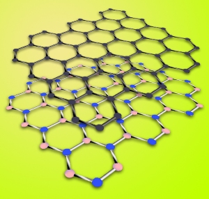
Groups headed by Alex Zettl and Michael Crommie from the Materials Sciences Division at Lawrence Berkeley National Laboratory (Berkeley Lab) of the U.S. Department of Energy and physics professors from the University of California at Berkeley have joined together to analyze the substrate candidates suitable for preserving the intrinsic properties of grapheme.
Study results on graphene’s interplay with a boron nitride substrate were recently published in Nano Letters.
Graphene is a 2D honeycomb of carbon and has a thickness of just one atom. Its electronic properties include low resistivity and high electron mobility. It is very sensitive to external conditions.
 Boron nitride’s attributes make it a better substrate for preserving graphene’s intrinsic properties
Régis Decker, the chief author of the Nano Letters, reported that the properties of grapheme can be influenced by any substrate. If someone wants to study the intrinsic properties of grapheme, then he/she has to work with suspended grapheme. But, suspended grapheme is not stable when examined with scanning probe methods such as scanning tunneling microscopy. Therefore, a technique has to be found in order to identify a substrate that can simulate the matter of suspended grapheme.
In October 2010, a group from Columbia University reported that grapheme mounted on a boron nitride substrate retained better electron mobility compared to grapheme supported on a silicon dioxide substrate. But their macroscopic measurements failed to answer many questions.
The Zettl and Crommie groups made a comparison between the two systems to identify why boron nitride works better than silicon dioxide.
Decker said that in order mimic suspended grapheme through a graphene-substrate system, the substrate requires a wide electronic band gap to shun any change that might occur in graphene’s electronic structure. The substrate also needs to be flat. Since boron nitride fulfills these requirements, it is a suitable candidate compared to silicon dioxide.
In order to develop graphene/BN devices, the group led by Zettl made boron nitride crystals into small flakes through the tried-and-true technique of shedding them between slips of Scotch Tape. Then the BN flakes were placed on a silicon dioxide layer. The doped silicon layer was utilized as a gate electrode to adjust the charge concentration during scanning tunneling microscopy.
Qiong Wu from the Crommie group developed grapheme through chemical vapor ousting on copper. The graphene sheets were changed to soft plastic from the copper and then fixed over the boron nitride flakes by constraining the soft plastic onto the BN. The graphene layer was rooted by placing a titanium gold electrode on the layer. Using these processes, three graphene/BN systems were developed.